LS013B4DN02 Sharp Microelectronics, LS013B4DN02 Datasheet - Page 12
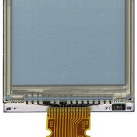
LS013B4DN02
Manufacturer Part Number
LS013B4DN02
Description
LCD Graphic Display Modules & Accessories 1.35 96x96 w/ FPC Mono Memory LCD
Manufacturer
Sharp Microelectronics
Datasheet
1.LS013B4DN02.pdf
(29 pages)
Specifications of LS013B4DN02
Pixel Density
96 x 96
Module Size (w X H X T)
28.2 mm x 32.34 mm x 1.4 mm
Viewing Area (w X H)
24.192 mm x 24.192 mm
Attached Touch Screen
No
Product
Graphic LCD Module
Interface
Serial
Operating Temperature Range
- 20 C to + 70 C
Lead Free Status / RoHS Status
Lead free / RoHS Compliant
Available stocks
Company
Part Number
Manufacturer
Quantity
Price
Company:

Part Number:
LS013B4DN02
Manufacturer:
SHARP
Quantity:
1 000


6-2) Power supply sequence
[Remark] Precaustions at ehte time of power on and power off.
VDD/VDDA(5V)
DISP
EXTCOMIN
SCS
Others
※Refer to timing chart and AC timing characteristics for detail
※1 ③ and ④ may be opposite (however, TCOM polarity inversion will not occur even with EXTCOMIN between
DISP= L . Also, when DISP and EXTCOMIN are simultaneously started up, allow 30us or more before SCS
starts up (It may be less than 60us).
※2 Setting value for pixel memory initialization
SCS=Driving accordingly to clear pixel internal memory method (use all clear flag or write all screen white)
S1=M2 (all clear flag) = “H” or write white
SCLK: Normal Driving
Remark 1)When power on , VDDand VDDA are same timem or VDD should be faster than the VDDA.
Remark 2) When power off, VDD and VDDA are same time or VDDA shoud be faster than the VDD.
[ON Sequence]
(1) 5V rise time (depends on IC)
(2) Pixel memory initialization T2: 1V or more Initialize with M2 (all clear flag) or write all screen white
(3) Release time for initialization of TCOM latch
(4) TCOM polarity initialization time
[Normal Operation]
Duration of normal driving
[Off Sequence]
(5) Pixel memory initialization time
(6) VA, VB, VCOM initialization time
(7) 5V falling time (Depends on IC)
Time required to release COM related latch circuit initialization which is initializing using DISP signals
Time required initializing TCOM polarity accordingly to EXTCOMIN input
GND
GND
GND
GND
GND
①
T1
※2
※2
On Sequence
②
T2
③※1 ④※1
T3
T4
SPEC No.
LCY-12T09303B
Normal operation
Normal operation
Normal operation
Normal operation
T5: 1V or more
T6: 1V or more
T4: 30us or more
T3: 30us or more
MODEL No.
※2
※2
⑤
T5
Off sequence
LS013B4DN02
⑥
T6
⑦
T7
GND
GND
GND
GND
GND
PAGE
11
Related parts for LS013B4DN02
Image
Part Number
Description
Manufacturer
Datasheet
Request
R

Part Number:
Description:
IC FLASH 32MBIT 110NS 56SSOP
Manufacturer:
Sharp Microelectronics
Datasheet:

Part Number:
Description:
IC FLASH 16MBIT 100NS 56TSOP
Manufacturer:
Sharp Microelectronics
Datasheet:

Part Number:
Description:
IC FLASH 64MBIT 120NS 56TSOP
Manufacturer:
Sharp Microelectronics
Datasheet:

Part Number:
Description:
IC FLASH 16MBIT 90NS 48TSOP
Manufacturer:
Sharp Microelectronics
Datasheet:
Part Number:
Description:
IC SRAM 16KBIT 100NS 24DIP
Manufacturer:
Sharp Microelectronics
Datasheet:
Part Number:
Description:
IC SRAM 16KBIT 100NS 24SOP
Manufacturer:
Sharp Microelectronics
Datasheet:
Part Number:
Description:
IC SRAM 64KBIT 100NS 28DIP
Manufacturer:
Sharp Microelectronics
Datasheet:
Part Number:
Description:
IC SRAM 64KBIT 100NS 28SOP
Manufacturer:
Sharp Microelectronics
Datasheet:
Part Number:
Description:
IC SRAM 64KBIT 100NS 28SOP
Manufacturer:
Sharp Microelectronics
Datasheet:
Part Number:
Description:
IC SRAM 256KBIT 70NS 28DIP
Manufacturer:
Sharp Microelectronics
Datasheet:
Part Number:
Description:
IC FLASH 8MBIT 90NS 48TSOP
Manufacturer:
Sharp Microelectronics
Datasheet:
Part Number:
Description:
IC FLASH 8MBIT 85NS 40TSOP
Manufacturer:
Sharp Microelectronics
Datasheet:
Part Number:
Description:
IC FLASH 8MBIT 85NS 40TSOP
Manufacturer:
Sharp Microelectronics
Datasheet:
Part Number:
Description:
IC FLASH 16MBIT 90NS 48TSOP
Manufacturer:
Sharp Microelectronics
Datasheet:
Part Number:
Description:
IC FLASH 16MBIT 70NS 56TSOP
Manufacturer:
Sharp Microelectronics
Datasheet: