TCET1100G Vishay, TCET1100G Datasheet - Page 4
TCET1100G
Manufacturer Part Number
TCET1100G
Description
Transistor Output Optocouplers Phototransistor Out Single CTR 50-600%
Manufacturer
Vishay
Specifications of TCET1100G
Isolation Voltage
5000 Vrms
Maximum Input Diode Current
60 mA
Maximum Reverse Diode Voltage
6 V
Output Device
Transistor
Output Type
DC
Configuration
1
Input Type
DC
Maximum Collector Emitter Voltage
70 V
Maximum Collector Emitter Saturation Voltage
300 mV
Current Transfer Ratio
600 %
Maximum Forward Diode Voltage
1.6 V
Maximum Collector Current
50 mA
Maximum Power Dissipation
265 mW
Maximum Operating Temperature
+ 100 C
Minimum Operating Temperature
- 40 C
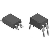
Package / Case
PDIP-4
No. Of Channels
1
Optocoupler Output Type
Phototransistor
Input Current
50mA
Output Voltage
70V
Opto Case Style
DIP
No. Of Pins
4
Mounting Type
Through Hole
Approval Bodies
VDE, CSA, BSI EN
Rohs Compliant
Yes
Lead Free Status / RoHS Status
Lead free / RoHS Compliant
Lead Free Status / RoHS Status
Lead free / RoHS Compliant, Lead free / RoHS Compliant
Available stocks
Company
Part Number
Manufacturer
Quantity
Price

Part Number:
TCET1100G
Manufacturer:
VISHAY/威世
Quantity:
20 000


TCET1100/TCET1100G
Vishay Semiconductors
Electrical Characteristics
T
Minimum and maximum values are testing requirements. Typical values are characteristics of the device and are the result of engineering
evaluation. Typical values are for information only and are not part of the testing requirements.
Input
Output
Coupler
Current Transfer Ratio
www.vishay.com
4
Forward voltage
Junction capacitance
Collector emitter voltage
Emitter collector voltage
Collector-emitter cut-off current
Collector emitter saturation
voltage
Cut-off frequency
Coupling capacitance
I
amb
C
/I
F
= 25 °C, unless otherwise specified
Parameter
Parameter
Parameter
Parameter
I
V
I
I
V
I
V
R
f = 1 MHz
V
V
V
F
C
E
F
R
CE
CE
CE
CE
CE
L
= 50 mA
= 10 mA, I
= 100 μA
= 1 mA
= 100 Ω
= 0 V, f = 1 MHz
= 20 V, I
= 5 V, I
= 5 V, I
= 5 V, I
= 5 V, I
Test condition
Test condition
Test condition
Test condition
F
F
F
F
C
f
= 10 mA,
= 1 mA
= 5 mA
= 10 mA
= 0, E = 0
= 1 mA
Symbol
Symbol
Symbol
TCET1101G
TCET1102G
TCET1103G
TCET1104G
TCET1100G
TCET1105G
TCET1106G
TCET1107G
TCET1108G
TCET1109G
TCET1101G
TCET1102G
TCET1103G
TCET1104G
V
V
V
TCET1101
TCET1102
TCET1103
TCET1104
TCET1100
TCET1105
TCET1106
TCET1107
TCET1108
TCET1109
TCET1101
TCET1102
TCET1103
TCET1104
I
CEO
CEsat
V
CEO
ECO
C
C
f
c
F
k
j
Part
Min
Min
Min
70
7
Symbol
CTR
CTR
CTR
CTR
CTR
CTR
CTR
CTR
CTR
CTR
CTR
CTR
CTR
CTR
1.25
Typ.
Typ.
Typ.
110
100
130
200
100
160
Min
0.3
50
10
13
22
34
56
50
50
80
40
63
Typ.
Document Number 83503
30
45
70
90
Max
Max
Max
100
1.6
0.3
Rev. 2.2, 05-Sep-06
Max
600
150
300
160
260
400
125
200
320
80
Unit
Unit
Unit
kHz
nA
pF
pF
V
V
V
V
Unit
%
%
%
%
%
%
%
%
%
%
%
%
%
%
Related parts for TCET1100G
Image
Part Number
Description
Manufacturer
Datasheet
Request
R

Part Number:
Description:
357-036-542-201 CARDEDGE 36POS DL .156 BLK LOPRO
Manufacturer:
Vishay
Datasheet:
Part Number:
Description:
357-036-542-201 CARDEDGE 36POS DL .156 BLK LOPRO
Manufacturer:
Vishay
Datasheet:
Part Number:
Description:
357-036-542-201 CARDEDGE 36POS DL .156 BLK LOPRO
Manufacturer:
Vishay
Datasheet:
Part Number:
Description:
357-036-542-201 CARDEDGE 36POS DL .156 BLK LOPRO
Manufacturer:
Vishay
Datasheet:
Part Number:
Description:
357-036-542-201 CARDEDGE 36POS DL .156 BLK LOPRO
Manufacturer:
Vishay
Datasheet:
Part Number:
Description:
357-036-542-201 CARDEDGE 36POS DL .156 BLK LOPRO
Manufacturer:
Vishay
Datasheet:
Part Number:
Description:
357-036-542-201 CARDEDGE 36POS DL .156 BLK LOPRO
Manufacturer:
Vishay
Datasheet:
Part Number:
Description:
357-036-542-201 CARDEDGE 36POS DL .156 BLK LOPRO
Manufacturer:
Vishay
Datasheet:
Part Number:
Description:
357-036-542-201 CARDEDGE 36POS DL .156 BLK LOPRO
Manufacturer:
Vishay
Datasheet:
Part Number:
Description:
357-036-542-201 CARDEDGE 36POS DL .156 BLK LOPRO
Manufacturer:
Vishay
Datasheet:
Part Number:
Description:
357-036-542-201 CARDEDGE 36POS DL .156 BLK LOPRO
Manufacturer:
Vishay
Datasheet:
Part Number:
Description:
357-036-542-201 CARDEDGE 36POS DL .156 BLK LOPRO
Manufacturer:
Vishay
Datasheet:
Part Number:
Description:
357-036-542-201 CARDEDGE 36POS DL .156 BLK LOPRO
Manufacturer:
Vishay
Datasheet:
Part Number:
Description:
357-036-542-201 CARDEDGE 36POS DL .156 BLK LOPRO
Manufacturer:
Vishay
Datasheet:
Part Number:
Description:
357-036-542-201 CARDEDGE 36POS DL .156 BLK LOPRO
Manufacturer:
Vishay
Datasheet: