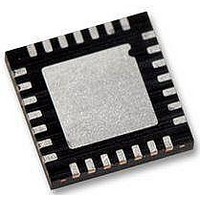
WM8986GECO/V Wolfson Microelectronics, WM8986GECO/V Datasheet - Page 18

WM8986GECO/V
Manufacturer Part Number
WM8986GECO/V
Description
Audio Amplifiers Class D Headphone DAC + Line Out
Manufacturer
Wolfson Microelectronics
Datasheet
1.WM8986GECOV.pdf
(88 pages)
Specifications of WM8986GECO/V
Product
Class-D
Output Power
40 mW
Thd Plus Noise
- 86 dB
Operating Supply Voltage
1.71 V to 3.6 V, 2.5 V to 3.6 V
Maximum Operating Temperature
+ 85 C
Mounting Style
SMD/SMT
Audio Load Resistance
16 Ohms
Minimum Operating Temperature
- 40 C
Output Signal Type
Differential
Supply Voltage (max)
3.6 V
Supply Voltage (min)
1.71 V, 2.5 V
Output Type
Differential
Package / Case
QFN-28
Lead Free Status / RoHS Status
Lead free / RoHS Compliant
WM8986
INTERNAL POWER ON RESET CIRCUIT
Figure 8 Typical Power up Sequence where AVDD1 is Powered before DCVDD
w
Figure 7 Internal Power on Reset Circuit Schematic
The WM8986 includes an internal Power-On-Reset Circuit, as shown in Figure 7, which is used to
reset the digital logic into a default state after power up. The POR circuit is powered from AVDD1
and monitors DCVDD. It asserts PORB low if AVDD1 or DCVDD is below a minimum threshold.
Figure 8 shows a typical power-up sequence where AVDD1 comes up first. When AVDD1 goes
above the minimum threshold, V
asserted low and the chip is held in reset. In this condition, all writes to the control interface are
ignored. Now AVDD1 is at full supply level. Next DCVDD rises to V
and all registers are in their default state and writes to the control interface may take place.
On power down, where AVDD1 falls first, PORB is asserted low whenever AVDD1 drops below the
minimum threshold V
pora_off
.
pora
, there is enough voltage for the circuit to guarantee PORB is
pord_on
and PORB is released high
PD, Rev 4.1, June 2009
Production Data
18


