WM8986GECO/V Wolfson Microelectronics, WM8986GECO/V Datasheet - Page 51
WM8986GECO/V
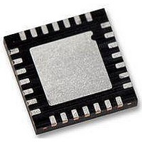
Manufacturer Part Number
WM8986GECO/V
Description
Audio Amplifiers Class D Headphone DAC + Line Out
Manufacturer
Wolfson Microelectronics
Datasheet
1.WM8986GECOV.pdf
(88 pages)
Specifications of WM8986GECO/V
Product
Class-D
Output Power
40 mW
Thd Plus Noise
- 86 dB
Operating Supply Voltage
1.71 V to 3.6 V, 2.5 V to 3.6 V
Maximum Operating Temperature
+ 85 C
Mounting Style
SMD/SMT
Audio Load Resistance
16 Ohms
Minimum Operating Temperature
- 40 C
Output Signal Type
Differential
Supply Voltage (max)
3.6 V
Supply Voltage (min)
1.71 V, 2.5 V
Output Type
Differential
Package / Case
QFN-28
Lead Free Status / RoHS Status
Lead free / RoHS Compliant


Production Data
w
In I
other bits up to the LSB are then transmitted in order. Depending on word length, BCLK frequency
and sample rate, there may be unused BCLK cycles between the LSB of one sample and the MSB of
the next.
Figure 29 I
In DSP/PCM mode, the left channel MSB is available on either the 1
rising edge of BCLK (selectable by LRP) following a rising edge of LRC. Right channel data
immediately follows left channel data. Depending on word length, BCLK frequency and sample rate,
there may be unused BCLK cycles between the LSB of the right channel data and the next sample.
In device master mode, the LRC output will resemble the LRC pulse shown in Figure 30 and Figure
31. In device slave mode, Figure 32 and Figure 33, it is possible to use any length of LRC pulse less
than 1/fs, providing the falling edge of the LRC pulse occurs greater than one BCLK period before the
rising edge of the next LRC pulse.
Figure 30 DSP/PCM Mode Audio Interface (mode A, LRP=0, Master)
Figure 31 DSP/PCM Mode Audio Interface (mode B, LRP=1, Master)
2
S mode, the MSB is available on the second rising edge of BCLK following a LRC transition. The
2
S Audio Interface (assuming n-bit word length)
st
(mode B) or 2
PD, Rev 4.1, June 2009
WM8986
nd
(mode A)
51
Related parts for WM8986GECO/V
Image
Part Number
Description
Manufacturer
Datasheet
Request
R

Part Number:
Description:
Manufacturer:
Wolfson Microelectronics
Datasheet: