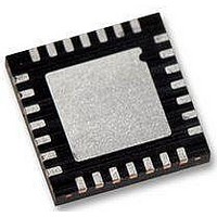
WM8986GECO/V Wolfson Microelectronics, WM8986GECO/V Datasheet - Page 67

WM8986GECO/V
Manufacturer Part Number
WM8986GECO/V
Description
Audio Amplifiers Class D Headphone DAC + Line Out
Manufacturer
Wolfson Microelectronics
Datasheet
1.WM8986GECOV.pdf
(88 pages)
Specifications of WM8986GECO/V
Product
Class-D
Output Power
40 mW
Thd Plus Noise
- 86 dB
Operating Supply Voltage
1.71 V to 3.6 V, 2.5 V to 3.6 V
Maximum Operating Temperature
+ 85 C
Mounting Style
SMD/SMT
Audio Load Resistance
16 Ohms
Minimum Operating Temperature
- 40 C
Output Signal Type
Differential
Supply Voltage (max)
3.6 V
Supply Voltage (min)
1.71 V, 2.5 V
Output Type
Differential
Package / Case
QFN-28
Lead Free Status / RoHS Status
Lead free / RoHS Compliant
Production Data
REGISTER BITS BY ADDRESS
w
0 (00h)
1 (01h)
2 (02h)
REGISTER
ADDRESS
[8:0]
8
7
6
5
4
3
2
1:0
8
7
6
5
4
3
2
1
0
BIT
RESET
OUT4MIXEN
OUT3MIXEN
PLLEN
BIASEN
BUFIOEN
VMIDSEL
ROUT1EN
LOUT1EN
SLEEP
BOOSTENR
BOOSTENL
INPPGAENR
INPPGAENL
Notes:
1. Default values of N/A indicate non-latched data bits (e.g. software reset or volume update bits).
2. Register bits marked as "Reserved" should not be changed from the default.
LABEL
N/A
0
0
0
0
0
0
0
00
0
0
0
0
0
0
0
0
0
DEFAULT
Software reset
Reserved
OUT4 mixer enable
0=disabled
1=enabled
OUT3 mixer enable
0=disabled
1=enabled
PLL enable
0=PLL off
1=PLL on
Reserved
Analogue amplifier bias control
0=disabled
1=enabled
Unused input/output tie off buffer enable
0=disabled
1=enabled
Reference string impedance to VMID pin
00= off (250kΩ VMID to AGND1)
01=75kΩ
10=300kΩ
11=5kΩ
ROUT1 output enable
0=disabled
1=enabled
LOUT1 output enable
0=disabled
1=enabled
0 = normal device operation
1 = residual current reduced in device standby
mode (Device must be in standby mode before
setting this bit)
Right channel Input BOOST enable
0 = Boost stage OFF
1 = Boost stage ON
Left channel Input BOOST enable
0 = Boost stage OFF
1 = Boost stage ON
Right channel input PGA enable
0 = disabled
1 = enabled
Left channel input PGA enable
0 = disabled
1 = enabled
Reserved
Reserved
DESCRIPTION
PD, Rev 4.1, June 2009
Resetting the
Chip
Analogue
Outputs
Power
Management
Power
Management
Master Clock
and Phase
Locked Loop
(PLL)
Power
Management
Power
Management
Power
Management
Power
Management
Power
Management
Power
Management
Power
Management
Power
Management
Power
Management
Power
Management
REFER TO
WM8986
67


