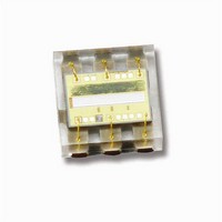
TSL2561CL TAOS, TSL2561CL Datasheet - Page 10

TSL2561CL
Manufacturer Part Number
TSL2561CL
Description
Light to Digital Converters Ambient Light Sensor Light to Digital
Manufacturer
TAOS
Datasheet
1.TSL2561T.pdf
(42 pages)
Specifications of TSL2561CL
Data Bus Width
20 bit
Peak Wavelength
640 nm, 940 nm
Maximum Operating Frequency
780 KHz
Operating Supply Voltage
2.7 V to 3.6 V
Operating Current
0.6 mA to 15 uA
Maximum Operating Temperature
+ 70 C
Minimum Operating Temperature
- 30 C
Interface Type
I2C
Maximum Fall Time
300 ns
Maximum Rise Time
300 ns
Mounting Style
SMD/SMT
Resolution
16 bit
Package / Case
Chip LED
Lead Free Status / RoHS Status
Lead free / RoHS Compliant
TSL2560, TSL2561
LIGHT-TO-DIGITAL CONVERTER
TAOS059N − MARCH 2009
Analog-to-Digital Converter
Digital Interface
NOTE: The Slave and SMB Alert Addresses are 7 bits. Please note the SMBus and I
SMBus and I
10
Copyright E 2009, TAOS Inc.
The TSL256x contains two integrating analog-to-digital converters (ADC) that integrate the currents from the
channel 0 and channel 1 photodiodes. Integration of both channels occurs simultaneously, and upon completion
of the conversion cycle the conversion result is transferred to the channel 0 and channel 1 data registers,
respectively. The transfers are double buffered to ensure that invalid data is not read during the transfer. After
the transfer, the device automatically begins the next integration cycle.
Interface and control of the TSL256x is accomplished through a two-wire serial interface to a set of registers
that provide access to device control functions and output data. The serial interface is compatible with System
Management Bus (SMBus) versions 1.1 and 2.0, and I
addresses that are selectable via an external pin (ADDR SEL). The slave address options are shown in Table 1.
Each Send and Write protocol is, essentially, a series of bytes. A byte sent to the TSL256x with the most
significant bit (MSB) equal to 1 will be interpreted as a COMMAND byte. The lower four bits of the COMMAND
byte form the register select address (see Table 2), which is used to select the destination for the subsequent
byte(s) received. The TSL256x responds to any Receive Byte requests with the contents of the register
specified by the stored register select address.
The TSL256X implements the following protocols of the SMB 2.0 specification:
D
D
D
D
D
D
D
The TSL256X implements the following protocols of the Philips Semiconductor I
D
D
be appended to the slave address by the master device to properly communicate with the TSL256X device.
Send Byte Protocol
Receive Byte Protocol
Write Byte Protocol
Write Word Protocol
Read Word Protocol
Block Write Protocol
Block Read Protocol
I
I
2
2
C Write Protocol
C Read (Combined Format) Protocol
2
C Protocols
ADDR SEL TERMINAL LEVEL
GND
Float
VDD
Table 1. Slave Address Selection
PRINCIPLES OF OPERATION
r
www.taosinc.com
SLAVE ADDRESS
0101001
1001001
0111001
2
C bus Fast-Mode. The TSL256x offers three slave
2
C protocols on pages 9 through 12. A read/write bit should
r
SMB ALERT ADDRESS
0001100
0001100
0001100
2
C specification:
The LUMENOLOGY r Company


