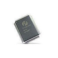
PI7C21P100BNHE Pericom Semiconductor, PI7C21P100BNHE Datasheet - Page 26

PI7C21P100BNHE
Manufacturer Part Number
PI7C21P100BNHE
Description
Peripheral Drivers & Components (PCIs) PCI-X to PCI-XBridge 2 Port
Manufacturer
Pericom Semiconductor
Datasheet
1.PI7C21P100BNHE.pdf
(79 pages)
Specifications of PI7C21P100BNHE
Maximum Operating Temperature
+ 70 C
Minimum Operating Temperature
0 C
Mounting Style
SMD/SMT
Operating Supply Voltage
3 V to 3.6 V
Package / Case
CSBGA-304
Lead Free Status / RoHS Status
Lead free / RoHS Compliant
Available stocks
Company
Part Number
Manufacturer
Quantity
Price
Company:
Part Number:
PI7C21P100BNHE
Manufacturer:
Pericom
Quantity:
135
Company:
Part Number:
PI7C21P100BNHE
Manufacturer:
PI
Quantity:
1 831
4.3.1
4.3.1.1
4.3.1.2
4.3.1.3
MEMORY READ TRANSACTIONS
Memory data is transferred from the originating side of PI7C21P100B to the destination side
using PCI memory read, memory read line, memory read multiple, PCI-X memory read
DWORD, and PCI-X memory read block transactions. All memory read transactions are
either delayed or split on the originating side of PI7C21P100B depending on the mode of the
originating side.
No translation is needed for these transactions.
The amount of data that is fetched is controlled by the downstream and upstream split
transaction control register. The split transaction capacity and split transaction commitment
limit fields control how much data is requested at any one time.
No translation is needed for these transactions.
Memory Read – Fetches only the requested DWORD if the command targets a non-
prefetchable memory space. Bits [25:24] offset 40h and bits [9:8] offset 40h control the mode
of prefetching for memory read transactions in the prefetchable range on the secondary and
primary bus respectively. The default is up to one cache line will be prefetched.
Memory Read Line – Bits [23:22] offset 40h and bits [7:6] offset 40h control the mode of
prefetching for memory read line transactions in the prefetchable range on the secondary and
primary bus respectively. The default is up to one cache line will be prefetched.
Memory Read Multiple – Bits [21:20] offset 40h and bits [5:4] offset 40h control the mode of
prefetching for memory read multiple transactions in the prefetchable range on the secondary
and primary bus respectively. The default is a full prefetch, limited to the value set by bits
[14:12] offset 40h. The default value is 512 bytes, or an entire read buffer.
PI7C21P100B must translate the conventional PCI memory read command to either the
memory read DWORD or the memory read block PCI-X Command. If the conventional PCI
memory read command targets non-prefetchable memory space, the command is translated
into a memory read DWORD. In any other instance, the conventional PCI memory read
command gets translated into a memory read block PCI-X command. Bits [25:24] offset 40h
and bits [9:8] offset 40h control the mode of prefetching for memory read transactions in the
prefetchable range on the secondary and primary bus respectively. The default is up to one
cache line will be prefetched. The default is up to one cache line will be prefetched.
Type 1 Configuration Read
PCI-X TO PCI-X
PCI TO PCI
PCI TO PCI-X
Type of Transaction
Page 26 of 79
Delayed/Split (PCI-X mode)
2-PORT PCI-X TO PCI-X BRIDGE
November 2005 – Revision 1.02
Type of Handling
PI7C21P100B


