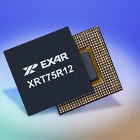
XRT75R12DIB-F Exar Corporation, XRT75R12DIB-F Datasheet - Page 26

XRT75R12DIB-F
Manufacturer Part Number
XRT75R12DIB-F
Description
Peripheral Drivers & Components (PCIs) 12 Channel 3.3V-5V temp -45 to 85C
Manufacturer
Exar Corporation
Datasheet
1.XRT75R12DIB-F.pdf
(133 pages)
Specifications of XRT75R12DIB-F
Maximum Operating Temperature
+ 85 C
Minimum Operating Temperature
- 40 C
Mounting Style
SMD/SMT
Operating Supply Voltage
3.3 V to 5 V
Package / Case
TBGA-420
Lead Free Status / RoHS Status
Lead free / RoHS Compliant
- Current page: 26 of 133
- Download datasheet (851Kb)
XRT75R12D
TWELVE CHANNEL E3/DS3/STS-1 LINE INTERFACE UNIT WITH SONET DESYNCHRONIZER
The Equalizer restores the integrity of the signal and compensates for the frequency dependent attenuation of
up to 900 feet of coaxial cable (1300 feet for E3). The Equalizer also boosts the high frequency content of the
signal to reduce Inter-Symbol Interference (ISI) so that the slicer slices the signal at 50% of peak voltage to
generate Positive and Negative data. The equalizer can be disabled by programming the appropriate register.
The Equalizer has two gain settings to provide optimum equalization. In the case of normally shaped DS3/
STS-1 pulses (pulses that meet the template requirements) that has been driven through 0 to 900 feet of cable,
the Equalizer can be enabled. However, for square-shaped pulses such as E3 or for DS3/STS-1 high pulses
(that does not meet the pulse template requirements), it is recommended that the Equalizer be disabled for
cable length less than 300 feet. This would help to prevent over-equalization of the signal and thus optimize
the performance in terms of better jitter transfer characteristics. The Equalizer also contains an additional 20
dB gain stage to provide the line monitoring capability (Receive Monitor Mode) of the resistively attenuated
signals which may have 20dB flat loss. The equalizer and the equalizer gain mode can be enabled by
programming the appropriate register. However, enabling the equalizer gain mode (Receive Monitor Mode)
suppresses the internal LOS circuitry and LOS will never assert nor LOS be declared when operating with
Receive Monitor Mode enabled.
N
The Clock and Data Recovery Circuit extracts the embedded clock, RxClk_n from the sliced digital data stream
and provides the retimed data to the B3ZS (HDB3) decoder. The Clock Recovery PLL can be in one of the
following two modes:
In the presence of input line signals on the RTIP_n and RRing_n input pins and when the frequency difference
between the recovered clock signal and the reference clock signal is less than 0.5%, the clock that is output on
the RxClk_n out pins is the Recovered Clock signal.
In the absence of input signals at RTIP_n and RRing_n pins, or when the frequency difference between the
recovered line clock signal and the reference clock applied on the ExClk_n input pins exceed 0.5%, a Loss of
Lock condition is declared by toggling RLOL_n output pin “High” or setting the RLOL_n bit to “1” in the control
register. Also, the clock output on the RxClk_n pins are the same as the reference channel clock.
F
3.3
3.4
3.3.1
3.4.1
3.4.2
OTE
IGURE
: The results of extensive testing indicate that even when the Equalizer was enabled, regardless of the cable length,
the integrity of the E3 signal was restored properly over 0 to 12 dB cable loss at Industrial Temperature.
7. ACG/E
Receive Equalizer
Clock and Data Recovery
Recommendations for Equalizer Settings
Data/Clock Recovery Mode
Training Mode
QUALIZER
B
LOCK
RRing_n
RTIP_n
D
IAGRAM
Equalizer
AGC/
22
Peak Detector
Detector
Slicer
LOS
REV. 1.0.3
Related parts for XRT75R12DIB-F
Image
Part Number
Description
Manufacturer
Datasheet
Request
R

Part Number:
Description:
Twelve Channel E3/ds3/sts-1 Line Interface Unit With Jitter
Manufacturer:
Exar Corporation
Datasheet:

Part Number:
Description:
BiCMOS Fixed, Quad, Voltage Output, Single or Dual Supply 8-Bit Digital-to-Analog Converter
Manufacturer:
Exar Corporation
Datasheet:

Part Number:
Description:
Manufacturer:
Exar Corporation
Datasheet:

Part Number:
Description:
Voltage-Controlled Oscillator
Manufacturer:
Exar Corporation
Datasheet:

Part Number:
Description:
INTEGRATED LINE TRANSMITTER
Manufacturer:
Exar Corporation
Datasheet:

Part Number:
Description:
Monolithic Function Generator
Manufacturer:
Exar Corporation
Datasheet:

Part Number:
Description:
CMOS Microprocessor Compatible Double-Buffered 12-Bit Digital-to-Analog Converter
Manufacturer:
Exar Corporation
Datasheet:

Part Number:
Description:
CMOS 6 BIT HIGH SPEED ANALOG TO DIGITAL CONVERTER
Manufacturer:
Exar Corporation
Datasheet:

Part Number:
Description:
Manufacturer:
Exar Corporation
Datasheet:

Part Number:
Description:
Manufacturer:
Exar Corporation
Datasheet:

Part Number:
Description:
8-Channel, Voltage Output 10 MHz Input Bandwidth 8-Bit Multiplying DACs with Serial Digital Data Por
Manufacturer:
Exar Corporation
Datasheet:

Part Number:
Description:
15 V CMOS Multiplying10-Bit Digital-to-Analog Converter
Manufacturer:
Exar Corporation
Datasheet:

Part Number:
Description:
Monolithic Function Generator
Manufacturer:
Exar Corporation
Datasheet:


