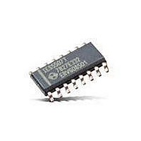
IES5507T Hendon Semiconductors, IES5507T Datasheet

IES5507T
Specifications of IES5507T
Available stocks
Related parts for IES5507T
IES5507T Summary of contents
Page 1
... IES5507 SCL 14 SDA 15 RESET 3 © 2009 Hendon Semiconductors Pty. Ltd. , all rights reserved. 2009 Mar 05, Revision 1.0 Buffered 4-Channel 2-Wire Bus Switch 3 GENERAL DESCRIPTION The IES5507 is a monolithic CMOS integrated circuit for 2-wire bus buffering and switching in applications including SMBus, PMbus, and other systems based on similar principles ...
Page 2
PINNING INFORMATION 5.1 Pin description SYMBOL PIN DESCRIPTION A0 1 Address Input Address Input 1 RESET 3 Active Low Reset Input SD0 4 Serial Data 0 SC0 5 Serial Clock 0 SD1 6 Serial Data 1 ...
Page 3
At some points during the communication, the data direction will reverse - for example, when the Slave transmits an acknowledge (ACK) or responds with it’s register contents. During these times, the controlling “input” side will have to rise to V ...
Page 4
The IES5507 is always addressable from the SCL/SDA side, regardless of the state of B7. Any device which can communicate data to the SCL/SDA pins, either by being directly attached to those pins or by transmitting through 7 BUS TRANSACTION ...
Page 5
LIMITING VALUES In accordance with the Absolute Maximum Rating System (IEC 134) Voltages are specified with respect to pin 8 (V SYMBOL PARAMETER V Supply voltage range ( Voltage range (SDA Sxx V Voltage range (RESET) RST ...
Page 6
SYMBOL PARAMETER RESET V HIGH-level input voltage RST(hi) V LOW-level input voltage RST(lo) V RESET Hysteresis RST(hys) I Input leakage current RST t LOW-level reset time w-RST(lo) t Reset (and POR) time RST Address A0, A1 HIGH-level input ...
Page 7
T = 25°C amb ( Fig.8 Typ.Input Levels vs. Supply Voltage 100 5. 2.7V ...
Page 8
APPLICATION INFORMATION 10.1 Design Considerations Figure 12 shows a typical data transfer through the IES5507. The IES5507 has excellent application to extending loads and expanding the address space of slave devices. Rise times are determined simply by the side ...
Page 9
Application circuits 3. SCL SDA Bus Master U3 400pF load @ 1MHz Master / or 4nF @ 100Hz Slave U4 SC2 SD2 400pF load @ 1MHz or 4nF @ 100Hz SC3 SD3 400pF load @ 1MHz or ...
Page 10
SCL SDA 2 Isolated I C Bus IES5507 provides bus isolation and simplifies calculation of bus RC components Fig.15 IES5507 isolating the standard I R1 180 V DD SCL SDA Bus Master ‘000’ U1 Structure in dashed box repeated ...
Page 11
... IES5507 T SO16 plastic small outline package; 16 leads; body width 3.9 mm Other package options are available - contact Hendon Semiconductors for details. For more information on packages, please refer to the document “Integrated Circuit Packaging and Soldering Information” on the Hendon Semiconductors web site. 12 ESD CAUTION Electrostatic Discharge (ESD) sensitive device ...
Page 12
... Exposure to limiting values for extended periods may affect device reliability. Application information Where application information is given advisory and does not form part of the specification. 15 COMPANY INFORMATION HENDON SEMICONDUCTORS PTY. LTD. ABN 17 080 879 616 Postal address: Hendon Semiconductors PO Box 2226 ...
Page 13
... DISCLAIMER Hendon Semiconductors Pty. Ltd. ABN 17 080 879 616 (“Hendon”) reserves the right to make changes to both its products and product data without notice. Hendon makes no warranty, representation or guarantee regarding the suitability of its products for any particular purpose, nor does Hendon assume any liability arising out of the use or application of any Hendon product. Hendon specifically disclaims any and all liability, including without limitation incidental or consequential damages ...


