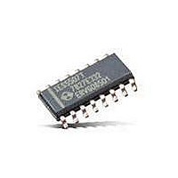
IES5507T Hendon Semiconductors, IES5507T Datasheet - Page 2

IES5507T
Manufacturer Part Number
IES5507T
Description
Buffers & Line Drivers Buffered 4-Chan Bus Switch
Manufacturer
Hendon Semiconductors
Datasheet
1.IES5507T.pdf
(13 pages)
Specifications of IES5507T
Logic Family
IES5507
Number Of Channels Per Chip
4
Supply Voltage (max)
7 V
Supply Voltage (min)
- 0.3 V
Maximum Operating Temperature
+ 85 C
Minimum Operating Temperature
- 40 C
Output Current
30 mA
Output Voltage
110 mV, 80 mV
Supply Current
0.1 uA
Lead Free Status / RoHS Status
Lead free / RoHS Compliant
Available stocks
Company
Part Number
Manufacturer
Quantity
Price
Company:
Part Number:
IES5507T
Manufacturer:
Hendon Semiconductors
Quantity:
135
5
5.1
6
6.1
The power supply voltage for the IES5507 may be any
voltage in the range 2.7 V to 5.5 V. The IC supply must be
common with the supply for the bus. Hysteresis on the
ports are a percentage of the IC’s power supply, hence
noise margin considerations should be taken into account
when selecting an operating voltage.
6.2
The clock signal buffer is uni-directional, with this pin
acting as the default input. However, the clock signal
direction may be reversed by setting the MSB of the
control register HIGH. In normal bus operations, for
example the I
uni-directional clock signal to the slave. For lowest cost the
IES5507 combines uni-directional buffering of the clock
signal with a bi-directional buffer for the data signal. Clock
stretching is therefore not supported and Slave devices
that may require clock stretching must be accommodated
by the Master adopting an appropriate clocking when
communicating with them.
2009 Mar 05, Revision 1.0
A0
A1
RESET
SD0
SC0
SD1
SC1
V
SD2
SC2
SD3
SC3
A2
SCL
SDA
V
SYMBOL
SS
DD
PINNING INFORMATION
FUNCTIONAL DESCRIPTION
Pin description
V
SCL - Clock Signal Input
DD
, V
2
1
2
3
4
5
6
7
8
9
10
11
12
13
14
15
16
SS
C bus, the Master device generates a
PIN
- DC supply pins
Address Input 0
Address Input 1
Active Low Reset Input
Serial Data 0
Serial Clock 0
Serial Data 1
Serial Clock 1
Negative supply (ground)
Serial Data 2
Serial Clock 2
Serial Data 3
Serial Clock 3
Address Input 2
Serial Clock Line (normally in)
Serial Data Line
Positive supply
DESCRIPTION
Buffered 4-Channel 2-Wire Bus Switch
2
5.2
The buffer includes hysteresis to ensure clean switching
signals are output, especially with slow rise times on high
capacitively loaded buses.
6.3
The clock signal from SCL is buffered through four
independent buffers, and the signal is presented at the four
SC0..3 ports. Ports are open-drain type and require
external pullup resistors.
When the MSB of the control register is set HIGH, the port
direction is reversed. The ‘AND-ed’ result of the four
SC0..3 lines is then used to drive the open drain output of
the SCL pin.
6.4
The data signal buffers are bi-directional. The port (SDA,
or any one of SD0..3) which first falls low, will decide the
direction of this buffer and “lock out” signals coming from
the opposite side. As the “input” signal continues to fall, it
will then drive the open-drain of the “output” side low.
Again, hysteresis is applied to the buffer to minimise the
effects of noise. Ports are open-drain type and require
external pullup resistors.
RESET
Pinning layout
SC0, SC1, SC2, SC3 - Clock Signal Outputs
SDA, SD0..3 - Data Signal Inputs/Outputs
SD0
SC0
SD1
SC1
V
A0
A1
SS
Fig.2 Pinning diagram (SO16)
1
2
3
4
5
6
7
8
IES5507
Product Specification
IES5507
16
15
14
13
12
11
10
9
pin5507-16
V
SDA
SCL
A2
SC3
SD3
SC2
SD2
DD


