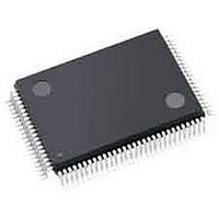
ispPAC-POWR1220AT8-02TN100I Lattice, ispPAC-POWR1220AT8-02TN100I Datasheet - Page 15

ispPAC-POWR1220AT8-02TN100I
Manufacturer Part Number
ispPAC-POWR1220AT8-02TN100I
Description
Current & Power Monitors & Regulators Prec. Power Supply Seq. Monitor Marg.
Manufacturer
Lattice
Series
ispPAC®r
Datasheet
1.ISPPAC-POWR1220AT8-02TN100I.pdf
(54 pages)
Specifications of ispPAC-POWR1220AT8-02TN100I
Mounting Style
SMD/SMT
Supply Voltage (max)
3.96 V
Supply Voltage (min)
2.8 V
Package / Case
TQFP-100
Applications
General Purpose
Voltage - Input
-0.3 V ~ 5.9 V
Voltage - Supply
2.8 V ~ 3.96 V
Current - Supply
40mA
Operating Temperature
-40°C ~ 85°C
Mounting Type
Surface Mount
Lead Free Status / RoHS Status
Lead free / RoHS Compliant
Available stocks
Company
Part Number
Manufacturer
Quantity
Price
Company:
Part Number:
ISPPAC-POWR1220AT8-02TN100I
Manufacturer:
Lattice
Quantity:
226
Company:
Part Number:
ISPPAC-POWR1220AT8-02TN100I
Manufacturer:
Lattice Semiconductor Corporation
Quantity:
10 000
Lattice Semiconductor
Figure 1-7. ispPAC-POWR1220AT8 Voltage Monitors
Figure 1-7 shows the functional block diagram of one of the 12 voltage monitor inputs - ‘x’ (where x = 1...12). Each
voltage monitor can be divided into three sections: Analog Input, Window Control, and Filtering. The first section
provides a differential input buffer to monitor the power supply voltage through VMONx+ (to sense the positive ter-
minal of the supply) and VMONxGS (to sense the power supply ground). Differential voltage sensing minimizes
inaccuracies in voltage measurement with ADC and monitor thresholds due to the potential difference between the
ispPAC-POWR1220AT8 device ground and the ground potential at the sensed node on the circuit board.
The voltage output of the differential input buffer is monitored by two individually programmable trip-point compara-
tors, shown as CompA and CompB. Table 1-1 shows all 368 trip points spanning the range 0.664V to 5.734V to
which a comparator’s threshold can be set.
Each comparator outputs a HIGH signal to the PLD array if the voltage at its positive terminal is greater than its pro-
grammed trip point setting, otherwise it outputs a LOW signal.
A hysteresis of approximately 1% of the setpoint is provided by the comparators to reduce false triggering as a
result of input noise. The hysteresis provided by the voltage monitor is a function of the input divider setting.
Table 1-3 lists the typical hysteresis versus voltage monitor trip-point.
AGOOD Logic Signal
All the VMON comparators auto-calibrate immediately after a power-on reset event. During this time, the digital
glitch filters are also initialized. This process completion is signalled by an internally generated logic signal:
AGOOD. All logic using the VMON comparator logic signals must wait for the AGOOD signal to become active.
Programmable Over-Voltage and Under-Voltage Thresholds
Figure 1-8 (a) shows the power supply ramp-up and ramp-down voltage waveforms. Because of hysteresis, the
comparator outputs change state at different thresholds depending on the direction of excursion of the monitored
power supply.
VMONxGS
VMONx
Input Buffer x
Differential
Trip Point A
Trip Point B
Analog Input
+
–
+
–
ispPAC-POWR1220AT8
Comp A
Comp B
1-15
Window Control
Comp A/Window
Select
ispPAC-POWR1220AT8 Data Sheet
Glitch
Glitch
Filter
Filter
Filtering
VMONxA
Signal
Logic
VMONxB
Signal
Logic
VMONx Status
I
2
To ADC
C Interface
Unit
Array
PLD


