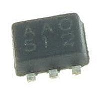
BD2270HFV-TR Rohm Semiconductor, BD2270HFV-TR Datasheet - Page 10

BD2270HFV-TR
Manufacturer Part Number
BD2270HFV-TR
Description
MOSFET & Power Driver ICs MOSFET Controller IC For Load Switching
Manufacturer
Rohm Semiconductor
Type
MOSFET Controller ICr
Specifications of BD2270HFV-TR
Package / Case
HVSOF-5
Product
MOSFET Gate Drivers
Rise Time
130 us
Fall Time
18 us
Supply Voltage (max)
5.5 V
Supply Voltage (min)
2.7 V
Supply Current
50 uA
Maximum Operating Temperature
+ 85 C
Mounting Style
SMD/SMT
Minimum Operating Temperature
- 25 C
Output Voltage
9.5 V
Primary Input Voltage
5.5V
No. Of Outputs
1
Voltage Regulator Case Style
HVSOF
No. Of Pins
5
Operating Temperature Range
-25°C To +85°C
Svhc
No SVHC (18-Jun-2010)
Base
RoHS Compliant
Lead Free Status / RoHS Status
Lead free / RoHS Compliant
Lead Free Status / RoHS Status
Lead free / RoHS Compliant
Available stocks
Company
Part Number
Manufacturer
Quantity
Price
●Thermal Derating Characteristics
Cautions on use
© 2009 ROHM Co., Ltd. All rights reserved.
BD2270HFV
www.rohm.com
(HVSOF5)
(1)
(2)
(3)
(4)
These conditions represent a range within which characteristics can be provided approximately as expected. The electrical
characteristics are guaranteed under the conditions of each parameter.
Furthermore, for all power supply terminals to ICs, mount a capacitor between the power supply and the GND terminal. At
the same time, in order to use an electrolytic capacitor, thoroughly check to be sure the characteristics of the capacitor to be
used present no problem including the occurrence of capacity dropout at a low temperature, thus determining the constant.
An excess in the absolute maximum ratings, such as supply voltage, temperature range of operating conditions, etc., can
break down devices, thus making impossible to identify breaking mode such as a short circuit or an open circuit. If any
special mode exceeding the absolute maximum ratings is assumed, consideration should be given to take physical safety
measures including the use of fuses, etc.
The reverse connection of power supply connector can break down ICs. Take protective measures against the breakdown
due to the reverse connection, such as mounting an external diode between the power supply and the IC’s power supply
terminal.
Design PCB pattern to provide low impedance for the wiring between the power supply and the GND lines. In this regard,
for the digital block power supply and the analog block power supply, even though these power supplies has the same level
of potential, separate the power supply pattern for the digital block from that for the analog block, thus suppressing the
diffraction of digital noises to the analog block power supply resulting from impedance common to the wiring patterns. For
the GND line, give consideration to design the patterns in a similar manner.
Absolute Maximum Ratings
Operating conditions
Reverse connection of power supply connector
Power supply line
800
700
600
500
400
300
200
100
0
0
25
Mounted on a 70 mm70 mm1.6 mm glass epoxy PCB
Fig. 39 Power dissipation curve (Pd-Ta Curve)
AMBIENT TEMPERATURE : Ta ( ℃ )
50
10/12
75
100
125
Technical Note
2009.04 - Rev.A
150


