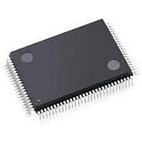
LC4256ZC-75TN100C Lattice, LC4256ZC-75TN100C Datasheet - Page 44

LC4256ZC-75TN100C
Manufacturer Part Number
LC4256ZC-75TN100C
Description
CPLD - Complex Programmable Logic Devices PROGRAMMABLE SUPER FAST HI DENSITY PLD
Manufacturer
Lattice
Datasheet
1.LC4256V-75TN100I.pdf
(94 pages)
Specifications of LC4256ZC-75TN100C
Memory Type
EEPROM
Number Of Macrocells
256
Number Of Product Terms Per Macro
80
Maximum Operating Frequency
200 MHz
Delay Time
4.5 ns
Number Of Programmable I/os
48
Operating Supply Voltage
1.8 V
Supply Current
0.341 mA
Maximum Operating Temperature
+ 90 C
Minimum Operating Temperature
0 C
Package / Case
TQFP-100
Mounting Style
SMD/SMT
Supply Voltage (max)
1.9 V
Supply Voltage (min)
1.7 V
Package
100TQFP
Family Name
ispMACH® 4000Z
Number Of Macro Cells
256
Maximum Propagation Delay Time
7.5 ns
Number Of User I/os
64
Number Of Logic Blocks/elements
36
Typical Operating Supply Voltage
1.8 V
Operating Temperature
0 to 90 °C
Lead Free Status / RoHS Status
Lead free / RoHS Compliant
Available stocks
Company
Part Number
Manufacturer
Quantity
Price
Company:
Part Number:
LC4256ZC-75TN100C
Manufacturer:
Lattice Semiconductor Corporation
Quantity:
10 000
Lattice Semiconductor
ispMACH 4000V/B/C/Z Power Supply and NC Connections
VCC
VCCO0
VCCO (Bank 0)
VCCO1
VCCO (Bank 1)
GND
GND (Bank 0)
GND (Bank 1)
NC
1. All grounds must be electrically connected at the board level. However, for the purposes of I/O current loading, grounds are associated with
2. Internal GNDs and I/O GNDs (Bank 0/1) are connected inside package.
3. V
4. Pin orientation follows the conventional order from pin 1 marking of the top side view and counter-clockwise.
5. ispMACH 4384V/B/C pin 46 is tied to GND (Bank 0).
6. ispMACH 4128V only.
7. Pin orientation A1 starts from the upper left corner of the top side view with alphabetical order ascending vertically and numerical order
8. ispMACH 4128Z and 4256Z only. NC for ispMACH 4064Z.
the bank shown.
ascending horizontally.
CCO
Signal
balls connect to two power planes within the package, one for V
P1, A14, B7, N8
G3, P5, C1
C5
M10, M14
A10, C13
B1, P2, N14, A13
E2, K2, N4, B4
N11, K13, E13, B11 55, 65, 82, 90
4064Z: C1, C3, E1,
E3, H2, J3, K1, M2,
M4, N5, P7, P8, M8,
P10, P11, P14, M12,
K14, K12, G13,
G14, E14, C13, B13,
B10, C10, A7, B5,
A5, A4, A1
4128Z: P8, A7
132-ball csBGA
8
8
, H12,
8
, M2
8
,
7
36, 57, 108, 129
3, 19, 34, 47, 136
64, 75, 91, 106, 119 78, 92, 110, 128,
1, 37, 73, 109
10, 18
137
118
4128V: 17, 20, 38,
45, 72, 89, 92, 110,
117, 144
4256V: 18, 90
144-pin TQFP
6
, 27, 46, 127,
6
, 99,
4
42, 69, 88, 130,
157, 176
4, 22, 40, 56, 166
144
2, 46
153
13, 31, 55, 155,
167
67, 79, 101, 119,
143
1, 43, 44, 45, 89,
131, 132, 133
44
176-pin TQFP
CCO0
5
, 65, 90, 134,
ispMACH 4000V/B/C/Z Family Data Sheet
and one for V
4
B2, B15, G8, G9, K8, K9, R2, R15
D6, F4, H7, J7, L4, N6
D11, F13, H10, J10, L13, N11
A1, A16, C6, C11, F3, F14, G7, G10, H8,
H9, J8, J9, K7, K10, L3, L14, P6, P11, T1,
T16
4256V/B/C, 128 I/O: A4, A5, A6, A11, A12,
A13, A15, B5, B6, B11, B12, B14, C7, D1,
D4, D5, D10, D12, D16, E1, E2, E4, E5, E7,
E10, E13, E14, E15, E16, F1, F2, F15, F16,
G1, G4, G5, G6, G12, G13, G14, J11, K3,
K4, K15, L1, L2, L12, L15, L16, M1, M2, M3,
M4, M5, M12, M13, M15, M16, N1, N2, N7,
N10, N12, N14, P5, P12, R4, R5, R6, R11,
R12, R16, T2, T4, T5, T6, T11, T12, T13, T15
4256V/B/C, 160 I/O: A5, A12, A15, B5, B6,
B11, B12, B14, D4, D5, D12, E1, E4, E5,
E13, E15, E16, F1, F2, F15, G1, G5, G12,
G14, L1, L2, L12, L15, L16, M1, M2, M3,
M12, M16, N1, N12, N14, P5, R4, R5, R6,
R11, R12, R16, T4, T5, T12, T15
4384V/B/C: B5, B12, D5, D12, E1, E15,
E16, F2, L12, M1, M2, M16, N12, R5, R12,
T4
4512V/B/C: None
CCO1
.
256-ball fpBGA
1
(Cont.)
2, 3, 7


