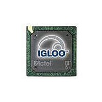
AGL030V5-VQG100 Actel, AGL030V5-VQG100 Datasheet - Page 138

AGL030V5-VQG100
Manufacturer Part Number
AGL030V5-VQG100
Description
FPGA - Field Programmable Gate Array 30K System Gates
Manufacturer
Actel
Datasheet
1.AGL030V2-CSG81.pdf
(236 pages)
Specifications of AGL030V5-VQG100
Processor Series
AGL030
Core
IP Core
Maximum Operating Frequency
892.86 MHz
Number Of Programmable I/os
79
Supply Voltage (max)
1.575 V
Maximum Operating Temperature
+ 70 C
Minimum Operating Temperature
0 C
Development Tools By Supplier
AGL-Icicle-Kit, AGL-Dev-Kit-SCS, Silicon-Explorer II, Silicon-Sculptor 3, SI-EX-TCA, FlashPro 4, FlashPro 3, FlashPro Lite
Mounting Style
SMD/SMT
Supply Voltage (min)
1.425 V
Number Of Gates
30 K
Package / Case
VQFP-100
Lead Free Status / RoHS Status
Lead free / RoHS Compliant
Available stocks
Company
Part Number
Manufacturer
Quantity
Price
Company:
Part Number:
AGL030V5-VQG100
Manufacturer:
RN2
Quantity:
522
Company:
Part Number:
AGL030V5-VQG100
Manufacturer:
Microsemi SoC
Quantity:
10 000
Company:
Part Number:
AGL030V5-VQG100I
Manufacturer:
Microsemi SoC
Quantity:
10 000
Part Number:
AGL030V5-VQG100I
Manufacturer:
MICROSEMI/美高森美
Quantity:
20 000
Company:
Part Number:
AGL030V5-VQG100IPR09
Manufacturer:
MICROSEMI
Quantity:
6 144
- Current page: 138 of 236
- Download datasheet (8Mb)
IGLOO DC and Switching Characteristics
Table 2-190 • RAM4K9
2- 12 4
Parameter
t
t
t
t
t
t
t
t
t
t
t
t
t
t
t
t
t
t
F
Note:
AS
AH
ENS
ENH
BKS
BKH
DS
DH
CKQ1
CKQ2
C2CWWL
C2CRWL
C2CWRH
RSTBQ
REMRSTB
RECRSTB
MPWRSTB
CYC
MAX
For specific junction temperature and voltage supply levels, refer to
Timing Characteristics
1.5 V DC Core Voltage
Address setup time
Address hold time
REN_B, WEN_B setup time
REN_B, WEN_B hold time
BLK_B setup time
BLK_B hold time
Input data (DI) setup time
Input data (DI) hold time
Clock High to new data valid on DO (output retained, WMODE = 0)
Clock High to new data valid on DO (flow-through, WMODE = 1)
Clock High to new data valid on DO (pipelined)
Address collision clk-to-clk delay for reliable write after write on same address - Applicable
to Closing Edge
Address collision clk-to-clk delay for reliable read access after write on same address -
Applicable to Opening Edge
Address collision clk-to-clk delay for reliable write access after read on same address -
Applicable to Opening Edge
RESET_B Low to data out Low on DO (flow-through)
RESET_B Low to data out Low on DO (pipelined)
RESET_B removal
RESET_B recovery
RESET_B minimum pulse width
Clock cycle time
Maximum frequency
Commercial-Case Conditions: T
J
= 70°C, Worst-Case VCC = 1.425 V
Description
R ev isio n 1 8
Table 2-6 on page 2-7
for derating values.
0.83
0.16
0.81
0.16
1.65
0.16
0.71
0.36
3.53
3.06
1.81
0.23
0.35
0.41
2.06
2.06
0.61
3.21
0.68
6.24
Std. Units
160
MHz
ns
ns
ns
ns
ns
ns
ns
ns
ns
ns
ns
ns
ns
ns
ns
ns
ns
ns
ns
ns
Related parts for AGL030V5-VQG100
Image
Part Number
Description
Manufacturer
Datasheet
Request
R

Part Number:
Description:
PQFP 100/FPGA, 768 CLBS, 30000 GATES, 108 MHz
Manufacturer:
Actel

Part Number:
Description:
FPGA - Field Programmable Gate Array 30K System Gates
Manufacturer:
Actel

Part Number:
Description:
FPGA - Field Programmable Gate Array 30K System Gates IGLOO
Manufacturer:
Actel
Datasheet:

Part Number:
Description:
FPGA - Field Programmable Gate Array 30K System Gates
Manufacturer:
Actel
Datasheet:

Part Number:
Description:
FPGA - Field Programmable Gate Array 30K System Gates
Manufacturer:
Actel
Datasheet:

Part Number:
Description:
FPGA - Field Programmable Gate Array 30K SYSTEM GATES
Manufacturer:
Actel


