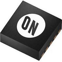
NCV8537MN250R2G ON Semiconductor, NCV8537MN250R2G Datasheet

NCV8537MN250R2G
Specifications of NCV8537MN250R2G
Available stocks
Related parts for NCV8537MN250R2G
NCV8537MN250R2G Summary of contents
Page 1
NCV8537 500 mA High Accuracy Low Dropout Linear Regulator, with Power Good Function The NCV8537 is a high performance low dropout linear voltage regulator. Based on the popular NCV8535, the device retains all the best features of its predecessor which ...
Page 2
OFF SENSE GND PWRG R1 1.0 mF 100k PWRG Figure 1. Typical Fixed Version Application Schematic OFF ...
Page 3
Vin Voltage Enable SD Reference Block NR NCV8537 Adjustable GND Figure 3. Block Diagram, Adjustable Output Version Vin Voltage Enable SD Reference Block NR NCV8537 Fix GND Figure 4. Block Diagram, Fixed Output Version Comp. Current and Series Pass Error ...
Page 4
PIN FUNCTION DESCRIPTION Pin No. Pin Name Regulated output voltage. Bypass to ground with C out 3 SENSE/ADJ For output voltage sensing, connect to Pins 1 and 2.at Fixed output Voltage version Adjustable pin at Adjustable output ...
Page 5
ELECTRICAL CHARACTERISTICS − 1.8 V Characteristic Output Voltage (Accuracy 500 mA load Output Voltage (Accuracy 2 5 0.1 mA ...
Page 6
ELECTRICAL CHARACTERISTICS − 2.5 V Characteristic Output Voltage (Accuracy 500 mA load Output Voltage (Accuracy 2 6 0.1 mA ...
Page 7
ELECTRICAL CHARACTERISTICS − 3.3 V Note 8) Characteristic Output Voltage (Accuracy 500 mA load Output Voltage (Accuracy 3 7.3 V, ...
Page 8
ELECTRICAL CHARACTERISTICS − Note 10) Characteristic Output Voltage (Accuracy 500 mA load Output Voltage (Accuracy 5 7.3 V, ...
Page 9
ELECTRICAL CHARACTERISTICS − ADJUSTABLE otherwise noted, Note 12) Characteristic Reference Voltage (Accuracy 500 mA out load Reference Voltage (Accuracy 2 ...
Page 10
OUT 1.83 1.82 1.81 1 1.8 V OUT 1.79 1.78 1.77 1.76 1.75 −40 − TEMPERATURE (°C) A Figure 5. Output Voltage ...
Page 11
T , TEMPERATURE (°C) A Figure 11. Dropout Voltage vs. Temperature 3.3 V Version 1000 900 I 800 sc 700 ...
Page 12
1.8 V OUT 0.0 3.6 3.4 3 INPUT VOLTAGE (V) IN Figure 17. Output Current Capability for the ...
Page 13
Figure 24. Power Good Activation Data Sheet Test Conditions, in 25° Capacitance 10 Unstable Area 5.0 Stable Area 0 0 100 200 300 OUTPUT CURRENT (mA) Figure 26. Stability with ESR vs. Output Current NOTE: ...
Page 14
Reverse Bias Protection Reverse bias is a condition caused when the input voltage goes to zero, but the output voltage is kept high either by a large output capacitor or another source in the application which feeds the output pin. ...
Page 15
... ORDERING INFORMATION Device Nominal Output Voltage NCV8537MN180R2G NCV8537MN250R2G NCV8537MN330R2G NCV8537MN500R2G NCV8537MNADJR2G †For information on tape and reel specifications, including part orientation and tape sizes, please refer to our Tape and Reel Packaging Specifications Brochure, BRD8011/D. *Please contact factory for other voltage options. Marking 1 ...
Page 16
... Pb−Free strategy and soldering details, please download the ON Semiconductor Soldering and Mounting Techniques Reference Manual, SOLDERRM/D. N. American Technical Support: 800−282−9855 Toll Free USA/Canada Europe, Middle East and Africa Technical Support: Phone: 421 33 790 2910 Japan Customer Focus Center Phone: 81− ...


