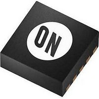
NCV8537MN250R2G ON Semiconductor, NCV8537MN250R2G Datasheet - Page 7

NCV8537MN250R2G
Manufacturer Part Number
NCV8537MN250R2G
Description
Low Dropout (LDO) Regulators LDO
Manufacturer
ON Semiconductor
Datasheet
1.NCV8537MN180R2G.pdf
(16 pages)
Specifications of NCV8537MN250R2G
Number Of Outputs
1
Input Voltage Max
16 V
Output Voltage
2.5 V
Output Type
Fixed
Dropout Voltage (max)
340 mV
Output Current
700 mA
Load Regulation
0.04 mV/mA
Voltage Regulation Accuracy
+/- 0.9 %
Maximum Operating Temperature
+ 125 C
Mounting Style
SMD/SMT
Minimum Operating Temperature
- 40 C
Package / Case
DFN10
Primary Input Voltage
12V
Output Voltage Fixed
2.5V
Dropout Voltage Vdo
340mV
No. Of Pins
10
Voltage Regulator Case Style
DFN
Operating Temperature Range
-40°C To +125°C
Rohs Compliant
Yes
Lead Free Status / RoHS Status
Lead free / RoHS Compliant
Available stocks
Company
Part Number
Manufacturer
Quantity
Price
Company:
Part Number:
NCV8537MN250R2G
Manufacturer:
ON Semiconductor
Quantity:
2 400
8. Performance guaranteed over the operating temperature range by design and/or characterization, production tested at T
9. Can be disabled per customer request.
ELECTRICAL CHARACTERISTICS − 3.3 V
Note 8)
Output Voltage (Accuracy) V
Output Voltage (Accuracy)
Output Voltage (Accuracy)
Line Regulation
Load Regulation
Dropout Voltage
Peak Output Current (See Figure 14)
Short Output Current (See Figure 14) V
Thermal Shutdown / Hysteresis
Ground Current
In Dropout
In Shutdown
Output Noise
Power Good Voltage
Power Good Pin Voltage Saturation (I
Power Good Pin Leakage
Power Good Blanking Time (Note 9)
Shutdown
SD Input Current, V
Output Current In Shutdown Mode, V
Reverse Bias Protection, Current Flowing from the Output Pin to GND
duty cycle pulse techniques are used during testing to maintain the junction temperature as close to ambient as possible.
V
V
V
V
I
I
I
I
In Regulation
C
C
Low Threshold
Hysteresis
High Threshold
Threshold Voltage ON
Threshold Voltage OFF
(V
V
load
load
load
load
in
in
in
in
nr
nr
in
in
I
I
I
I
V
V
= 3.7 V to 7.3 V, I
= 3.7 V to 7.3 V, I
= 3.7 V to 12 V, I
= 3.7 V, I
= 0 nF, I
= 10 nF, I
load
load
load
load
= 3.7 V to 7.3 V, I
= 0 V, V
= 500 mA
= 300 mA
= 50 mA
= 0.1 mA
in
SD
= 3.7 V, I
= 0 V
= 500 mA (Note 8)
= 300 mA
= 50 mA
= 0.1 mA
load
out_forced
load
load
load
= 500 mA, f = 10 Hz to 100 kHz, C
SD
= 0.1 mA to 500 mA
= 500 mA, f = 10 Hz to 100 kHz, C
= 0 V to 0.4 V or V
= 0.1 mA
load
load
load
load
= 3.3 V)
= 0.1 mA
= 0.1 mA to 500 mA, T
= 0.1 mA to 500 mA, T
in
= 0.1 mA to 500 mA, T
Characteristic
out
ef
in
= 1.0 mA)
= 0 V
< 7 V, T
SD
= 2.0 V to V
A
(V
A
A
= 25°C
A
out
= 25°C
= −40°C to +125°C
= 0°C to +85°C
out
out
= 3.3 V typical, V
in
http://onsemi.com
= 10 mF
= 10 mF
7
in
= 3.7 V, T
Load
Symbol
Line
I
V
I
I
GNDsh
V
I
I
OUTR
V
efleak
V
V
V
V
V
GND
OSD
noise
I
I
I
T
efdo
t
SD
DO
pk
sc
out
out
out
elft
ef
SD
J
A
Reg
Reg
= −40°C to +125°C, unless otherwise noted,
−0.90%
−1.40%
−1.50%
3.254
3.325
3.27
Min
500
93
2
160/10
0.04
0.04
0.07
0.07
Typ
340
230
700
200
110
3.3
3.3
3.3
4.6
0.8
10
69
46
95
97
50
10
9
−
2
1
0.90%
1.40%
1.50%
3.346
Max
3.33
3.35
800
900
220
500
7.5
2.5
0.4
14
99
1
1
1
J
= T
A
= 25°C. Low
mV/mA
mVrms
mV/V
Unit
% of
V
mV
mA
mA
mA
mV
mA
mA
mA
mA
mA
mA
mA
°C
ms
V
V
V
V
out


