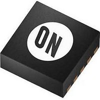
NCV8537MN250R2G ON Semiconductor, NCV8537MN250R2G Datasheet - Page 14

NCV8537MN250R2G
Manufacturer Part Number
NCV8537MN250R2G
Description
Low Dropout (LDO) Regulators LDO
Manufacturer
ON Semiconductor
Datasheet
1.NCV8537MN180R2G.pdf
(16 pages)
Specifications of NCV8537MN250R2G
Number Of Outputs
1
Input Voltage Max
16 V
Output Voltage
2.5 V
Output Type
Fixed
Dropout Voltage (max)
340 mV
Output Current
700 mA
Load Regulation
0.04 mV/mA
Voltage Regulation Accuracy
+/- 0.9 %
Maximum Operating Temperature
+ 125 C
Mounting Style
SMD/SMT
Minimum Operating Temperature
- 40 C
Package / Case
DFN10
Primary Input Voltage
12V
Output Voltage Fixed
2.5V
Dropout Voltage Vdo
340mV
No. Of Pins
10
Voltage Regulator Case Style
DFN
Operating Temperature Range
-40°C To +125°C
Rohs Compliant
Yes
Lead Free Status / RoHS Status
Lead free / RoHS Compliant
Available stocks
Company
Part Number
Manufacturer
Quantity
Price
Company:
Part Number:
NCV8537MN250R2G
Manufacturer:
ON Semiconductor
Quantity:
2 400
Reverse Bias Protection
goes to zero, but the output voltage is kept high either by a
large output capacitor or another source in the application
which feeds the output pin.
the output pin to input pin through the PN junction with
limited current capability and with the potential to destroy
the IC.
withstand up to 7.0 V on the output pin with virtually no
current flowing from output pin to input pin, and only
negligible amount of current (tens of mA) flowing from the
output pin to ground for infinite duration.
Input Capacitor
recommended to improve the transient response of the
regulator and/or if the regulator is located more than a few
inches from the power source. It will also reduce the circuit’s
sensitivity to the input line impedance at high frequencies.
The capacitor should be mounted with the shortest possible
track length directly across the regular’s input terminals.
Output Capacitor
as long as it fulfills its 1.0 mF requirement. There are no
constraints on the minimum ESR and it will remain stable up
to an ESR of 5.0 W. Larger capacitor values will improve the
noise rejection and load transient response.
Noise Reduction Pin
capacitor (C
(see Figure 1). In applications where very low noise is not
required, the noise reduction pin can be left unconnected.
Dropout Voltage
output voltage.
Thermal Considerations
integrated circuit in the event that the maximum junction
Reverse bias is a condition caused when the input voltage
Normally in a bipolar LDO all the current will flow from
Due to an improved architecture, the NCV8537 can
An input capacitor of at least 1.0 mF, any type, is
The NCV8537 remains stable with any type of capacitor
Output noise can be greatly reduced by connecting a 10 nF
The voltage dropout is measured at 97% of the nominal
Internal thermal limiting circuitry is provided to protect the
nr
) between the noise reduction pin and ground
APPLICATIONS INFORMATION
http://onsemi.com
14
temperature is exceeded. This feature provides protection
from a catastrophic device failure due to accidental
overheating. This protection feature is not intended to be used
as a substitute to heat sinking. The maximum power that can
be dissipated, can be calculated with the equation below:
for the DFN package option. The DFN package includes an
exposed metal pad that is specifically designed to reduce the
junction to air thermal resistance, R
Adjustable Operation
as shown in Figure 2 with a range of 1.25 to 10 V. The
appropriate resistor divider can be found by solving the
equation below. The recommended current through the
resistor divider is from 10 mA to 100 mA. This can be
accomplished by selecting resistors in the kW range. As
result, the I
can be ignored.
Power Good Operation
logic Low when it drops below the nominal output voltage.
Refer to the electrical characteristics for the threshold values
at which point the Power Good goes Low. When the
NCV8537 is above the nominal output voltage, the
Power Good will remain at logic High.
between V
approximately 100 kW is recommended to minimize the
current consumption. No pullup resistor is required if the
Power Good output is not being used. The Power Good does
not function during thermal shutdown and when the part is
disabled.
For improved thermal performance, contact the factory
The output voltage can be set by using a resistor divider
The Power Good pin on the NCV8537 will produce a
The external pullup resistor needs to be connected
V
adj
in
out
* R2 becomes negligible in the equation and
and the Power Good pin. A resistor of
+ 1.25 * (1 ) R3 R2) ) I
P D +
T J(max) * T A
R qJA
qJA
.
adj
* R2
(eq. 1)
(eq. 2)


