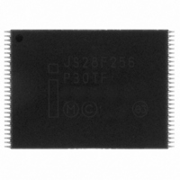
JS28F256P30TFA NUMONYX, JS28F256P30TFA Datasheet - Page 45

JS28F256P30TFA
Manufacturer Part Number
JS28F256P30TFA
Description
IC FLASH 256MBIT 110NS 56TSOP
Manufacturer
NUMONYX
Series
Axcell™r
Datasheet
1.PF48F4000P0ZBQEF.pdf
(94 pages)
Specifications of JS28F256P30TFA
Format - Memory
FLASH
Memory Type
FLASH
Memory Size
256M (16Mx16)
Speed
110ns
Interface
Parallel
Voltage - Supply
1.7 V ~ 2 V
Operating Temperature
-40°C ~ 85°C
Package / Case
56-TSOP
Package
56TSOP
Cell Type
NOR
Density
256 Mb
Architecture
Sectored
Block Organization
Asymmetrical
Location Of Boot Block
Top
Typical Operating Supply Voltage
1.8 V
Sector Size
32KByte x 4|128KByte x 255
Timing Type
Asynchronous|Synchronous
Interface Type
Parallel|Serial
Lead Free Status / RoHS Status
Lead free / RoHS Compliant
Other names
902052
902052
JS28F256P30TF 902052
902052
JS28F256P30TF 902052
Available stocks
Company
Part Number
Manufacturer
Quantity
Price
Company:
Part Number:
JS28F256P30TFA
Manufacturer:
MICRON
Quantity:
946
Part Number:
JS28F256P30TFA
Manufacturer:
MICRON/镁光
Quantity:
20 000
P30-65nm
Table 19: Burst Sequence Word Ordering (Sheet 2 of 2)
11.2.7
11.2.8
11.2.9
11.3
Datasheet
45
14
15
1
2
3
4
5
6
7
1
1
1
1
1
1
1
1
1
Clock Edge
The Clock Edge (CE) bit selects either a rising (default) or falling clock edge for CLK.
This clock edge is used at the start of a burst cycle, to output synchronous data, and to
assert/deassert WAIT.
Burst Wrap
The Burst Wrap (BW) bit determines whether 4-word, 8-word, or 16-word burst length
accesses wrap within the selected word-length boundaries or cross word-length
boundaries. When BW is set, burst wrapping does not occur (default). When BW is
cleared, burst wrapping occurs.
When performing synchronous burst reads with BW set (no wrap), an output delay may
occur when the burst sequence crosses its first device-row (16-word) boundary. If the
burst sequence’s start address is 4-word aligned, then no delay occurs. If the start
address is at the end of a 4-word boundary, the worst case output delay is one clock
cycle less than the first access Latency Count. This delay can take place only once, and
doesn’t occur if the burst sequence does not cross a device-row boundary. WAIT
informs the system of this delay when it occurs.
Burst Length
The Burst Length bits (BL[2:0]) select the linear burst length for all synchronous burst
reads of the flash memory array. The burst lengths are 4-word, 8-word, 16-word or
continuous.
Continuous-burst accesses are linear only, and do not wrap within any word length
boundaries (see
cycle begins, the device outputs synchronous burst data until it reaches the end of the
“burstable” address space.
One-Time-Programmable (OTP) Registers
The device contains 17 one-time programmable (OTP) registers that can be used to
implement system security measures and/or device identification. Each OTP register
can be individually locked.
The first 128-bit OTP Register is comprised of two 64-bit (8-word) segments. The lower
64-bit segment is pre-programmed at the Numonyx factory with a unique 64-bit
number. The upper 64-bit segment, as well as the other sixteen 128-bit OTP Registers,
1-2-3-4
2-3-4-5
3-4-5-6
Table 19, “Burst Sequence Word Ordering” on page
7-8-9-10-11-12-13-14
6-7-8-9-10-11-12-13
5-6-7-8-9-10-11-12
4-5-6-7-8-9-10-11
3-4-5-6-7-8-9-10
1-2-3-4-5-6-7-8
2-3-4-5-6-7-8-9
14-15-16-17-18…28-29
15-16-17-18-19…29-30
7-8-9-10-11…21-22
6-7-8-9-10…20-21
1-2-3-4-5…15-16
2-3-4-5-6…16-17
3-4-5-6-7…17-18
4-5-6-7-8…18-19
5-6-7-8-9…19-20
Order Number: 320002-10
14-15-16-17-18-19-20-
15-16-17-18-19-20-21-
44). When a burst
7-8-9-10-11-12-13…
6-7-8-9-10-11-12-…
5-6-7-8-9-10-11…
4-5-6-7-8-9-10…
1-2-3-4-5-6-7-…
2-3-4-5-6-7-8-…
3-4-5-6-7-8-9-…
…
…
Mar 2010


