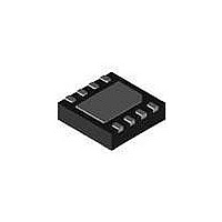
NCP5901MNTBG ON Semiconductor, NCP5901MNTBG Datasheet - Page 3

NCP5901MNTBG
Manufacturer Part Number
NCP5901MNTBG
Description
IC MOSFET DVR SYNC VR12 8-DFN
Manufacturer
ON Semiconductor
Type
VR12 Compatible Synchronous Buck MOSFET Driverr
Datasheet
1.NCP5901DR2G.pdf
(9 pages)
Specifications of NCP5901MNTBG
Configuration
High and Low Side, Synchronous
Input Type
Non-Inverting
Delay Time
25ns
Number Of Configurations
1
Number Of Outputs
2
Mounting Type
Surface Mount
Package / Case
8-DFN
Product
MOSFET Gate Drivers
Propagation Delay Time
25 ns
Mounting Style
SMD/SMT
Number Of Drivers
1
Output Voltage
35 V
Lead Free Status / RoHS Status
Lead free / RoHS Compliant
Current - Peak
-
High Side Voltage - Max (bootstrap)
-
Voltage - Supply
-
Operating Temperature
-
Lead Free Status / Rohs Status
Lead free / RoHS Compliant
Available stocks
Company
Part Number
Manufacturer
Quantity
Price
Company:
Part Number:
NCP5901MNTBG
Manufacturer:
ON Semiconductor
Quantity:
1 400
Part Number:
NCP5901MNTBG
Manufacturer:
ON/安森美
Quantity:
20 000
Stresses exceeding Maximum Ratings may damage the device. Maximum Ratings are stress ratings only. Functional operation above the
Recommended Operating Conditions is not implied. Extended exposure to stresses above the Recommended Operating Conditions may affect
device reliability.
* The maximum package power dissipation must be observed.
1. I in
2. Operation at −40°C to −10°C guaranteed by design, not production tested.
12V_POWER
Table 2. ABSOLUTE MAXIMUM RATINGS
Table 3. THERMAL INFORMATION
DRON
PWM
Symbol
2
T
R
MSL
TP4
Cu, 1 oz thickness.
T
STG
T
qJA
A
J
1.02
Pin Symbol
1uF
C5
R1
DRVH
DRVL
PWM
GND
VCC
BST
SW
EN
Thermal Characteristic
Operating Junction Temperature Range (Note 2)
Operating Ambient Temperature Range
Maximum Storage Temperature Range
Moisture Sensitivity Level
R143
0.0
CR1
MMSD4148
BST
PWM
EN
VCC
NCP5901
R164
0.0
PAD
GND
SW
HG
LG
C4
TP8
TP3
0.027uF
(All signals referenced to AGND unless noted otherwise)
DRVH and DRVL Control Input
VREG_SW1_HG
VREG_SW1_OUT
VREG_SW1_LG
Main Supply Voltage Input
(Bootstrap Supply Return)
Bootstrap Supply Voltage
High Side Driver Output
TP6
Low Side Driver Output
Parameter
Switching Node
Figure 3. Application Circuit
Enable Pin
Pin Name
Ground
TP7
http://onsemi.com
SOIC Package (Note 1)
DFN Package (Note 1)
Q9
NTMFS4851N
R142
0.0
3
SOIC Package
DFN Package
TP2
TP5
TP1
Q10
NTMFS4851N
40 V ≤ 50 ns wrt/ GND
35 V wrt/ GND
15 V wrt/ SW
Q1
NTMFS4821N
40 V ≤ 50 ns
VCC+0.3 V
BST+0.3 V
V
6.5 V
6.5 V
15 V
35 V
0 V
MAX
R3
2.2
C6
2700pF
−10 to +125
−55 to +150
0 to 150
Value
123
74
4.7uF
1
1
C1
235nH
L
−2 V (<200 ns) wrt/SW
4.7uF
C2
−5 V (<200 ns)
−10 V (200 ns)
−0.3 V wrt/SW
−0.3 V wrt/SW
JP13_ETCH
JP14_ETCH
−0.3 V DC
−0.3 V
−0.3 V
−0.3 V
V
−5 V
0 V
4.7uF
MIN
C3
°C/W
Unit
°C
°C
°C
+
390uF
CSN11
CSP11
VCCP
CE9


