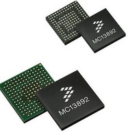
MC13892BJVL Freescale Semiconductor, MC13892BJVL Datasheet - Page 69

MC13892BJVL
Manufacturer Part Number
MC13892BJVL
Description
IC PMU I.MX51/37/35/27 186MAPBGA
Manufacturer
Freescale Semiconductor
Datasheets
1.MC13892AJVLR2.pdf
(156 pages)
2.MC13892AJVLR2.pdf
(2 pages)
3.MC13892AJVLR2.pdf
(16 pages)
4.MC13892AJVLR2.pdf
(5 pages)
Specifications of MC13892BJVL
Applications
Battery Management, Display (LED Drivers), Handheld/Mobile Devices, Power Supply
Operating Temperature
-40°C ~ 85°C
Mounting Type
Surface Mount
Package / Case
186-LFBGA
Mounting Style
SMD/SMT
Duty Cycle (max)
55 %
Input Voltage
- 0.3 V to + 20 V
Maximum Operating Temperature
+ 85 C
Minimum Operating Temperature
- 30 C
Output Current
30 mA
Output Voltage
3.3 V
Topology
Boost
Lead Free Status / RoHS Status
Lead free / RoHS Compliant
Current - Supply
-
Voltage - Supply
-
Lead Free Status / Rohs Status
Lead free / RoHS Compliant
Available stocks
Company
Part Number
Manufacturer
Quantity
Price
Company:
Part Number:
MC13892BJVL
Manufacturer:
Freescale Semiconductor
Quantity:
10 000
Company:
Part Number:
MC13892BJVLR2
Manufacturer:
Freescale Semiconductor
Quantity:
10 000
EXITING FROM LOW POWER OFF MODES
Standby voltage set points until the applicable time slot of the startup sequencer. At that point, the respective switcher is updated
for the PUMSx defined default state for mode and voltage. Subsequent closing of the power gate switches will be coordinated
by software to complete restoration of the full system power tree.
POWER GATING SPECIFICATIONS AND CONTROL
is isolated (or power gated) from its loading on the other side of the switch. The power gate drive outputs are SPI controlled in
the active modes as shown in
Analog Integrated Circuit Device Data
Freescale Semiconductor
Table 37. Power Gating Characteristics
Notes
54.
55.
Output Voltage V
Turn-on Time
Turn Off Time
Average Bias Current
PWGTx Input Voltage
DC Load Current
Load Capacitance
When a Turn On event occurs, any switchers that are active through Low Power Off modes will stay in PFM mode at their
A power gate driver pulled low may be thought of as power gating being active since this is the condition where a power source
Larger capacitive loading values will lead to longer turn on times exceeding the given limits; smaller values will lead to larger ripple at
the output.
Input supply is assumed in the range of 3.0 < BP < 4.65 V; lower BP values may extend turn on time, and functionality not supported
for BP less than ~2.7 V.
Parameter
(54),
OUT
Table 38. Power Gate Drive State Control
(55)
(54)
Off
Cold Start
Warm Start
Watchdog, On, User Off Wait
User Off, Memory Hold, Internal Memory Hold Power Cut
Table
Output High
Output Low
Enable to V
Disable to V
t > 500 μs after Enable
NMOS drain voltage
At PWGTDRVx output
Used as a condition for the other parameters
38.
OUT
OUT
Mode
= V
< 1.0 V
Condition
Figure 14. Memory Hold Circuit
OUTMIN
-250 mV
Min
PWGTDRV1
SPI Controlled
5.0
0.6
0.5
-
-
-
-
-
L
Low
Low
Low
ow
Typ
5.40
1.0
50
-
-
-
-
-
FUNCTIONAL DEVICE OPERATION
PWGTDRV2
SPI Controlled
Low
Low
Low
Low
Max
5.70
100
100
100
2.0
1.0
OPERATING MODES
1
5
Units
mV
μA
nA
nF
μs
μs
V
V
13892
69


