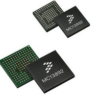
MC13892BJVL Freescale Semiconductor, MC13892BJVL Datasheet - Page 78

MC13892BJVL
Manufacturer Part Number
MC13892BJVL
Description
IC PMU I.MX51/37/35/27 186MAPBGA
Manufacturer
Freescale Semiconductor
Datasheets
1.MC13892AJVLR2.pdf
(156 pages)
2.MC13892AJVLR2.pdf
(2 pages)
3.MC13892AJVLR2.pdf
(16 pages)
4.MC13892AJVLR2.pdf
(5 pages)
Specifications of MC13892BJVL
Applications
Battery Management, Display (LED Drivers), Handheld/Mobile Devices, Power Supply
Operating Temperature
-40°C ~ 85°C
Mounting Type
Surface Mount
Package / Case
186-LFBGA
Mounting Style
SMD/SMT
Duty Cycle (max)
55 %
Input Voltage
- 0.3 V to + 20 V
Maximum Operating Temperature
+ 85 C
Minimum Operating Temperature
- 30 C
Output Current
30 mA
Output Voltage
3.3 V
Topology
Boost
Lead Free Status / RoHS Status
Lead free / RoHS Compliant
Current - Supply
-
Voltage - Supply
-
Lead Free Status / Rohs Status
Lead free / RoHS Compliant
Available stocks
Company
Part Number
Manufacturer
Quantity
Price
Company:
Part Number:
MC13892BJVL
Manufacturer:
Freescale Semiconductor
Quantity:
10 000
Company:
Part Number:
MC13892BJVLR2
Manufacturer:
Freescale Semiconductor
Quantity:
10 000
FUNCTIONAL DEVICE OPERATION
SUPPLIES
DYNAMIC VOLTAGE SCALING
processor. SW1 and SW2 allow for three different set points with controlled transitions to avoid sudden output voltage changes,
which could cause logic disruptions on their loads. Preset operating points for SW1 and SW2 can be set up for:
• Normal operation: output value selected by SPI bits SWx[4:0]. Voltage transitions initiated by SPI writes to SWx[4:0] are
• DVS: output can be higher or lower than normal operation for tailoring to application requirements. Configured by SPI bits
• Standby (Deep Sleep): can be higher or lower than normal operation, but is typically selected to be the lowest state retention
78
13892
To reduce overall power consumption, processor core voltages can be varied depending on the mode or activity level of the
governed by the same DVS stepping rate that is programmed for DVSx pin initiated transitions.
SWxDVS[4:0] and controlled by a DVSx pin transition.
voltage of a given process. Set by SPI bits SWxSTBY[4:0] and controlled by a Standby event (STANDBY logically and'd with
STANDBYSEC). Voltage transitions initiated by Standby are governed by the same DVS stepping that is programmed for
DVSx pin initiated transitions.
The following tables summarize the set point control and DVS time stepping applied to SW1 and SW2.
100 %
100 %
100 %
90 %
80 %
70 %
60 %
50 %
40 %
30 %
20 %
10 %
90 %
80 %
70 %
60 %
50 %
40 %
30 %
20 %
10 %
90 %
80 %
70 %
60 %
50 %
40 %
30 %
20 %
10 %
0 %
0 %
0 %
0
0
0
1 0
1 0
1 0
S W1 P WM Pu lse S kip pi ng mo de E ffi ciency Vo ut = 0, 725 V
S W2 P WM Pu lse S kip pi ng mo de E ffi ciency Vo ut = 1. 250 V
S W4 P WM Pu lse S kip pi ng mo de E ffi ciency Vo ut = 1. 800 V
20
20
20
3 0
3 0
3 0
40
40
40
Table 49. DVS Control Logic Table for SW1 and SW2
Ilo a d (m A)
Ilo a d (m A)
Ilo a d (m A)
Notes
60.
50
50
50
STANDBY
Figure 19. Buck Switcher PWM (Pulse Skipping) Efficiency
60
60
60
STANDBY is the logical anding of STANDBY and STANDBYSEC
0
0
1
70
70
70
(60)
80
80
80
90
90
90
DVSx Pin
10 0
10 0
10 0
X
0
1
Vin = 3 ,00 0 V
Vin = 3 ,60 0 V
Vin = 4 ,65 0 V
Vin = 3 ,00 0 V
Vin = 3 ,60 0 V
Vin = 4 ,65 0 V
Vin = 3 ,00 0 V
Vin = 3 ,60 0 V
Vin = 4 ,65 0 V
SWx[4:0]
SWxDVS[4:0]
SWxSTBY[4:0]
100 %
100 %
100 %
90 %
80 %
70 %
60 %
50 %
40 %
30 %
20 %
10 %
90 %
80 %
70 %
60 %
50 %
40 %
30 %
20 %
10 %
90 %
80 %
70 %
60 %
50 %
40 %
30 %
20 %
10 %
0 %
0 %
0 %
Set Point Selected by
0
0
0
50 1 00 150 200 25 0 300 35 0 4 00 450 50 0 55 0 6 00 650 70 0 7 50 800 85 0 90 0 9 50 10 0
50
50
1 00 1 50 20 0 25 0 300
1 00 1 50 20 0 2 50 30 0 35 0 400
S W1 PWM P ulse Ski ppi ng mo de E ffi ciency Vo ut = 0, 725 V
S W2 P WM Pu lse S kip pin g m od e E ffici ency V ou t = 1.250 V
S W4 PWM P ulse Ski ppi ng mo de E ffi ciency Vo ut = 1. 800 V
350 4 00 4 50 50 0 55 0 600
Il oa d (m A)
Ilo a d (m A)
Il oa d (m A)
Analog Integrated Circuit Device Data
450 5 00 5 50 60 0 65 0 700
650 7 00 7 50 80 0 85 0 900
Freescale Semiconductor
750 8 00
850 9 00
0
1 05
0
Vin = 3, 000 V
Vin = 3, 600 V
Vin = 4, 650 V
Vin = 3,0 00 V
Vin = 3,6 00 V
Vin = 4,6 50 V
Vin = 3,0 00 V
Vin = 3,6 00 V
Vin = 4,6 50 V


