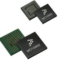
MC13892BJVL Freescale Semiconductor, MC13892BJVL Datasheet - Page 88

MC13892BJVL
Manufacturer Part Number
MC13892BJVL
Description
IC PMU I.MX51/37/35/27 186MAPBGA
Manufacturer
Freescale Semiconductor
Datasheets
1.MC13892AJVLR2.pdf
(156 pages)
2.MC13892AJVLR2.pdf
(2 pages)
3.MC13892AJVLR2.pdf
(16 pages)
4.MC13892AJVLR2.pdf
(5 pages)
Specifications of MC13892BJVL
Applications
Battery Management, Display (LED Drivers), Handheld/Mobile Devices, Power Supply
Operating Temperature
-40°C ~ 85°C
Mounting Type
Surface Mount
Package / Case
186-LFBGA
Mounting Style
SMD/SMT
Duty Cycle (max)
55 %
Input Voltage
- 0.3 V to + 20 V
Maximum Operating Temperature
+ 85 C
Minimum Operating Temperature
- 30 C
Output Current
30 mA
Output Voltage
3.3 V
Topology
Boost
Lead Free Status / RoHS Status
Lead free / RoHS Compliant
Current - Supply
-
Voltage - Supply
-
Lead Free Status / Rohs Status
Lead free / RoHS Compliant
Available stocks
Company
Part Number
Manufacturer
Quantity
Price
Company:
Part Number:
MC13892BJVL
Manufacturer:
Freescale Semiconductor
Quantity:
10 000
Company:
Part Number:
MC13892BJVLR2
Manufacturer:
Freescale Semiconductor
Quantity:
10 000
FUNCTIONAL DEVICE OPERATION
BATTERY INTERFACE AND CONTROL
charger or a USB host can be connected. It can also support dead battery operation and unregulated chargers.
CHARGE PATH
CHARGER LINE UP
voltage, and as the regulated supply voltage to the application in case of a dead battery operation. In order to support dead
battery operation, a so called “serial path” charging configuration including M3 needs to be used. Then in case of a dead battery,
the transistor M3 is made non-conducting and the internal trickle charge current charges the battery. If the battery is sufficiently
charged, the transistor M3 is made conducting which connects the battery to the application just like during normal operation
without a charger. In so called single path charging, M3 is replaced by a short and the pin BATTFET must be floating. Dead
battery operation is not supported in this case. Transistors M1 and M2 become non-conducting if the charger voltage is too high.
The VBUS must be shorted to CHRGRAW in cases where the wall charger and VBUS voltages are contained on a common pin.
A current can be supplied from the battery to an accessory with all transistors M1, M2, and M3 conducting, by enabling the
reverse supply mode. An unregulated wall charger configuration can be built, in which case CHRGSE1B must be pulled low. The
battery current monitoring resistor R1 and the charge LED indicator are optional. More detail on the battery current monitoring
can be found in
The preferred device for M3 is the On Semiconductor NTHS2101P for its low R
CHARGER SIGNALS
interrupts.
chapter and the SPI bit summary in
88
13892
The battery management interface is optimized for applications with a single charger connector to which a standard wall
The charge path is depicted in the following diagram.
Transistors M1 and M2 control the charge current and provide voltage regulation. The latter is used as the top off change
The preferred devices for M1 and M2 are Fairchild™ FDZ193P, due to their small package outline and thermal characteristics.
The charger uses a number of thresholds for proper operation and will also signal various events to the processor through
Table 61
ADC
summarizes the main signals given, including the control bits. For details see the related sections in this
Subsystem.
BATTERY INTERFACE AND CONTROL
SPI
Bitmap.
Figure 26. Charge Path Block Diagram
DSON
and small footprint.
Analog Integrated Circuit Device Data
Freescale Semiconductor


