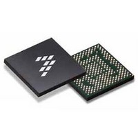
SC900841JVKR2 Freescale Semiconductor, SC900841JVKR2 Datasheet - Page 146

SC900841JVKR2
Manufacturer Part Number
SC900841JVKR2
Description
IC POWER MGT 338-MAPBGA
Manufacturer
Freescale Semiconductor
Specifications of SC900841JVKR2
Applications
PC's, PDA's
Operating Temperature
-40°C ~ 85°C
Mounting Type
Surface Mount
Package / Case
338-TBGA
Input Voltage
2.8 V to 4.4 V
Maximum Operating Temperature
+ 85 C
Minimum Operating Temperature
- 40 C
Lead Free Status / RoHS Status
Lead free / RoHS Compliant
Current - Supply
-
Voltage - Supply
-
Lead Free Status / Rohs Status
Lead free / RoHS Compliant
Available stocks
Company
Part Number
Manufacturer
Quantity
Price
Company:
Part Number:
SC900841JVKR2
Manufacturer:
Freescale Semiconductor
Quantity:
10 000
- Current page: 146 of 192
- Download datasheet (8Mb)
ground, which avoids using coupling capacitors for
connecting a headset. The amplifiers are supplied from CPIN
= 1.8 V while a single stage negative charge pump provides
the CPOUT = -1.8 V supply rail. The charge pump is enabled
when one of the headset amplifiers get enabled. The charge
pump input pin (CPIN) can be connect to the internal VDDQ
buck regulator in the application. In that case, VDDQ must be
enabled prior to the headset amplifier, to ensure proper
headset operation.
HEADPHONE/HEADSET DETECTION
push to talk button switch is done through the MIC2BIAS
circuit (MC2B and MC2IN pins) in the 900841. A basic
detection that there is an accessory attached to the system is
146
Table 93. Amplifiers Ahsr and Ahsl Performance Specifications
Table 94. Line Out Performance Specifications
900841
FUNCTIONAL DEVICE OPERATION
AUDIO
Notes
Amplifier Bias Current
THD
PSRR
Noise
Startup Time
Isolation
Channel Separation
Load-impedance
30.
Single Ended Output Swing
Gain
Amplifier Bias Current
THD
PSRR
Noise
Startup Time
Isolation
Channel Separation
Load Impedance
The outputs of the amplifiers are driven relative to true
The accessory detection of a headset, headphone or a
Applies for Ahsr and Ahsl activated individually and simultaneously with CPIN=1.8 V
Parameter
Per Channel from CPIN
Output 2.0 V
Relative to BP
Input referred
Including charge pump
Not routed
Output 2.0 V
Relative to BP
Input referred
Per channel
Condition
Not routed
PP
, 32 Ω
PP
STEREO LINE OUT
RXOUTL. These outputs can be used for instance to route
the audio to an accessory connected to a bottom connector,
such as for a docking station with playback speakers. These
outputs are enabled by setting the PCCNTLOR and
PSCNTLOL bits.
enabled even when MIC2BIAS is off (MIC2BIAS=0) in order
to save system power. After a first detection is made, the
firmware must enable MIC2BIAS in order to detect what kind
of accessory or to detect between long or short button
switches.
The audio can be routed to the line-outs RXOUTR and
Minimum
-0.5
2.0
90
80
10
-
-
-
-
-
12.8
90
80
-
-
-
-
-
Typical
100
200
0
Analog Integrated Circuit Device Data
-
-
-
-
-
-
-
750
1.0
32
-
-
-
-
Maximum
Freescale Semiconductor
0.5
-60
-75
10
-
-
-
-
-
-60
8.0
-75
-
-
-
-
-
μ VrmsA
μ VrmsA
Units
dBA
V
dBA
dB
μ A
dB
dB
dB
k Ω
us
ms
μ A
dB
dB
dB
PP
Ω
Related parts for SC900841JVKR2
Image
Part Number
Description
Manufacturer
Datasheet
Request
R
Part Number:
Description:
Ultra-mobile Platform Pmic
Manufacturer:
Freescale Semiconductor, Inc
Datasheet:

Part Number:
Description:
Sc900 Programmable Penta Uldo With Reset And I2c Interface
Manufacturer:
Semtech Corporation
Datasheet:
Part Number:
Description:
Manufacturer:
Freescale Semiconductor, Inc
Datasheet:
Part Number:
Description:
Manufacturer:
Freescale Semiconductor, Inc
Datasheet:
Part Number:
Description:
Manufacturer:
Freescale Semiconductor, Inc
Datasheet:
Part Number:
Description:
Manufacturer:
Freescale Semiconductor, Inc
Datasheet:
Part Number:
Description:
Manufacturer:
Freescale Semiconductor, Inc
Datasheet:
Part Number:
Description:
Manufacturer:
Freescale Semiconductor, Inc
Datasheet:
Part Number:
Description:
Manufacturer:
Freescale Semiconductor, Inc
Datasheet:
Part Number:
Description:
Manufacturer:
Freescale Semiconductor, Inc
Datasheet:
Part Number:
Description:
Manufacturer:
Freescale Semiconductor, Inc
Datasheet:
Part Number:
Description:
Manufacturer:
Freescale Semiconductor, Inc
Datasheet:
Part Number:
Description:
Manufacturer:
Freescale Semiconductor, Inc
Datasheet:
Part Number:
Description:
Manufacturer:
Freescale Semiconductor, Inc
Datasheet:
Part Number:
Description:
Manufacturer:
Freescale Semiconductor, Inc
Datasheet:


