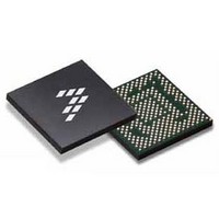
SC900841JVKR2 Freescale Semiconductor, SC900841JVKR2 Datasheet - Page 73

SC900841JVKR2
Manufacturer Part Number
SC900841JVKR2
Description
IC POWER MGT 338-MAPBGA
Manufacturer
Freescale Semiconductor
Specifications of SC900841JVKR2
Applications
PC's, PDA's
Operating Temperature
-40°C ~ 85°C
Mounting Type
Surface Mount
Package / Case
338-TBGA
Input Voltage
2.8 V to 4.4 V
Maximum Operating Temperature
+ 85 C
Minimum Operating Temperature
- 40 C
Lead Free Status / RoHS Status
Lead free / RoHS Compliant
Current - Supply
-
Voltage - Supply
-
Lead Free Status / Rohs Status
Lead free / RoHS Compliant
Available stocks
Company
Part Number
Manufacturer
Quantity
Price
Company:
Part Number:
SC900841JVKR2
Manufacturer:
Freescale Semiconductor
Quantity:
10 000
- Current page: 73 of 192
- Download datasheet (8Mb)
VDDQ
Buck PWM voltage-mode control DC/DC regulator.
the load conditions. These modes can be set through the SPI
and include a PFM mode, an Automatic Pulse Skipping
mode, and a PWM mode.
Main Features
• Uses the V
• It is used as a pre-regulator to many LDO rails, for
• Uses Integrated MOSFETs
• 4.0 MHz switching frequency
• High efficiency operating modes depending on load
Analog Integrated Circuit Device Data
Freescale Semiconductor
This is a 4.0 MHz fully integrated 2-switch synchronous
The switcher can operate in different modes depending on
enhanced efficiency and reduced thermal dissipation. It
also supplies power to rails in the CPU (central processing
unit), Platform controller hub, and the platform
conditions
PWR
rail as its power supply
V
DDQ
C
ODDQ
C
INDDQ
V
PWR
L
DDQ
PGNDDDQ
PVINDDQ
SWDDQ
Figure 27. VDDQ Detailed Internal Block Diagram
FBDDQ
Figure 28. VDDQ Efficiency Curves
V
Internal
Compensation
REF
I
Z1
SENSE 5
Driver
EA
Z2
Controller
shutting down.
ADC, and stored in a register for the processor to access.
The peak current is sensed internally for over-current
protection purposes. If an over-current condition is detected,
the regulator will limit the current through a cycle by cycle
operation and alert the system through the VDDQFAULT
signal, which will in turn assert the VRFAULT Interrupt signal.
• Output can be discharged through the low side switch.
• Peak current sensing with over-current protection
• Uses internal compensation
• Gate drive circuits are supplied directly from VPWR
Efficiency Curves
mode, based on the recommended external component
values and typical output voltage of 1.8 V. 3.0 V ≤ VPWR ≤
4.4 V.
VDDQ will be discharged every time the regulator is
The output current is measured internally, digitized by the
The following efficiency curves are calculated under PWM
AOACCTLVDDQ
VDDQFAULT
CTLVDDQ
FUNCTIONAL DEVICE OPERATION
Interface
SPI
POWER SUPPLIES
900841
73
Related parts for SC900841JVKR2
Image
Part Number
Description
Manufacturer
Datasheet
Request
R
Part Number:
Description:
Ultra-mobile Platform Pmic
Manufacturer:
Freescale Semiconductor, Inc
Datasheet:

Part Number:
Description:
Sc900 Programmable Penta Uldo With Reset And I2c Interface
Manufacturer:
Semtech Corporation
Datasheet:
Part Number:
Description:
Manufacturer:
Freescale Semiconductor, Inc
Datasheet:
Part Number:
Description:
Manufacturer:
Freescale Semiconductor, Inc
Datasheet:
Part Number:
Description:
Manufacturer:
Freescale Semiconductor, Inc
Datasheet:
Part Number:
Description:
Manufacturer:
Freescale Semiconductor, Inc
Datasheet:
Part Number:
Description:
Manufacturer:
Freescale Semiconductor, Inc
Datasheet:
Part Number:
Description:
Manufacturer:
Freescale Semiconductor, Inc
Datasheet:
Part Number:
Description:
Manufacturer:
Freescale Semiconductor, Inc
Datasheet:
Part Number:
Description:
Manufacturer:
Freescale Semiconductor, Inc
Datasheet:
Part Number:
Description:
Manufacturer:
Freescale Semiconductor, Inc
Datasheet:
Part Number:
Description:
Manufacturer:
Freescale Semiconductor, Inc
Datasheet:
Part Number:
Description:
Manufacturer:
Freescale Semiconductor, Inc
Datasheet:
Part Number:
Description:
Manufacturer:
Freescale Semiconductor, Inc
Datasheet:
Part Number:
Description:
Manufacturer:
Freescale Semiconductor, Inc
Datasheet:


