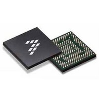
SC900841JVKR2 Freescale Semiconductor, SC900841JVKR2 Datasheet - Page 41

SC900841JVKR2
Manufacturer Part Number
SC900841JVKR2
Description
IC POWER MGT 338-MAPBGA
Manufacturer
Freescale Semiconductor
Specifications of SC900841JVKR2
Applications
PC's, PDA's
Operating Temperature
-40°C ~ 85°C
Mounting Type
Surface Mount
Package / Case
338-TBGA
Input Voltage
2.8 V to 4.4 V
Maximum Operating Temperature
+ 85 C
Minimum Operating Temperature
- 40 C
Lead Free Status / RoHS Status
Lead free / RoHS Compliant
Current - Supply
-
Voltage - Supply
-
Lead Free Status / Rohs Status
Lead free / RoHS Compliant
Available stocks
Company
Part Number
Manufacturer
Quantity
Price
Company:
Part Number:
SC900841JVKR2
Manufacturer:
Freescale Semiconductor
Quantity:
10 000
OVERVIEW
between the PMIC solution and the rest of the system.
• SPI interface: This is the serial communications interface
• Communications (COMMs) Module Interface: This is the
• Interrupt controller
• Sideband signals: These are I/O signals between the
• I
• Freescale chip set communications signals: This includes
• Special registers
SPI INTERFACE
host controller to access the register set. Using these
registers, 900841 resources can be controlled. The registers
provide information on the PMIC status, as well as
information on external signals.
data bits each. The map is not fully populated. A detailed
structure of the register set along with bit names, positions,
and basic descriptions, are given in
descriptions are included in the individual functional sections
for application guidance.
individual sub-circuit descriptions and the
determine the read/write capability of each bit.
Analog Integrated Circuit Device Data
Freescale Semiconductor
This section addresses the various interfaces and I/Os
System control interface includes the following:
between the 900841and the System Control Unit (SCU) in
the platform controller hub.
interface between the various basic and advanced
communication modules, and the PMIC solution. It
consists of two components:
• A Serial Communications port (Mini-SPI): This port
• Dedicated I/O signals for direct COMMs control of the
900841 and the Ultra-mobile Platform architecture for
control and status reporting.
control and status reporting signal between the 900841
and the companion chip, 900842 in Freescale’s power
management solution.
The 900841 contains a SPI interface port, which allows a
The addressable register map spans 1024 registers of 8
Note that not all bits are truly writable. Refer to the
2
S Bus Interface for Audio/Voice
goes to the 900841 PMIC, which houses the digital core
supply of the COMMs module.
PMIC solution.
Figure 5. SPI Read from PMIC Diagram (One Address/Data Packet shown)
Table
FUNCTIONAL DEVICE OPERATION
116. Expanded bit
Table 116
SYSTEM CONTROL INTERFACE
to
Table 6. SPI Interface Pin Functionality
is the slave. The SPI interface operates at a typical frequency
of 12.5 MHz, and at a maximum frequency of 25 MHz, with
lower speeds supported.
active high (CPOL = 0), and data is latched on the falling
edge of clock (CPHA = 1). The chip select signal, SPICSB,
is active low. The SPICSB line must remain active during the
entire SPI transfer. The MISO line will be tri-stated while
SPICSB is high.
bit address code (MSB first), 5 "dead" bits and 8 data bits
(also MSB first). The Read/Write bit selects whether the SPI
transaction is a read or a write: for a write operation, the R/W
bit must be a one; for a read operation, it must be a zero.
address bits is ignored. The MISO pin will output the data
field pointed to by the 10-bit address loaded at the beginning
of the SPI sequence. SPI read backs of the address field and
unused bits are returned as zero. For read operations, the
PMIC supports address auto-increment.
data is transferred into the registers on the falling edge of the
24th clock cycle. All unused SPI bits in each register must be
written to a zero.
inactive and then active again. After the LSB of data is sent,
if the SPICSB line is held low, up to seven additional address/
data packets may be sent as writes to the PMIC. Refer to the
VRCOMP Pin
SPI Read Protocol, and SPI Timing.
The Platform controller hub is the master, while the PMIC
The SPI interface is configured in mode 1: clock polarity is
The SPI frame consists of 24 bits: a Read/Write bit, a 10-
For a read transaction, any data on the MOSI pin after the
For a write operation, once all the data bits are written, the
To start a new SPI transfer, the SPICSB line must go
The following diagrams illustrate the SPI Write Protocol,
Pin Name
SPICSB
SPIVCC
SPICLK
MOSI
MISO
section.
Master In / Slave Out (Serial Data Out)
Master Out / Slave In (Serial Data In)
SPI Clock Input (up to 25 MHz)
FUNCTIONAL DEVICE OPERATION
SPI Bus Supply - 1.8 V typical
SYSTEM CONTROL INTERFACE
Chip Select (Active Low)
SPI Functionality
900841
41


