CP2112EK Silicon Laboratories Inc, CP2112EK Datasheet - Page 13
CP2112EK
Manufacturer Part Number
CP2112EK
Description
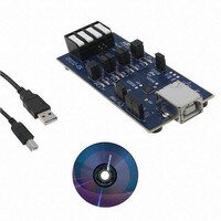
KIT EVAL FOR CP2112
Manufacturer
Silicon Laboratories Inc
Specifications of CP2112EK
Main Purpose
Interface, USB 2.0 to SMBus Bridge
Embedded
No
Utilized Ic / Part
CP2112
Primary Attributes
Full Speed (12Mbps)
Secondary Attributes
LED Status Indicators
Interface Type
USB
Operating Supply Voltage
3.3 V
Product
Interface Development Tools
For Use With/related Products
CP2112
Lead Free Status / RoHS Status
Lead free / RoHS Compliant
Lead Free Status / RoHS Status
Lead free / RoHS Compliant
Other names
336-2010
Available stocks
Company
Part Number
Manufacturer
Quantity
Price
Company:

Part Number:
CP2112EK
Manufacturer:
Silicon Labs
Quantity:
135


6.2. SMBus Operation
Two types of data transfers are possible: data transfers from a master transmitter to an addressed slave receiver
(WRITE) and data transfers from an addressed slave transmitter to a master receiver (READ). The master device
initiates both types of data transfers and provides the serial clock pulses on SCL. The SMBus interface on the
CP2112 operates as a master, but also has a configurable slave address associated with it that the CP2112 will
only ACK upon receiving. Multiple master devices on the same bus are supported. If two or more masters attempt
to initiate a data transfer simultaneously, an arbitration scheme is employed with a single master always winning
the arbitration. Note that it is not necessary to specify one device as the Master in a system; any device that
transmits a START and a slave address becomes the master for the duration of that transfer.
A typical SMBus transaction consists of a START condition followed by an address byte (Bits7–1: 7-bit slave
address; Bit0: R/W direction bit), one or more bytes of data, and a STOP condition. Bytes that are received (by a
master or slave) are acknowledged (ACK) with a low SDA during a high SCL (see Figure 6). If the receiving device
does not ACK, the transmitting device will read a NACK (not acknowledge), which is a high SDA during a high
SCL.
The direction bit (R/W) occupies the least-significant bit position of the address byte. The direction bit is set to logic
1 to indicate a "READ" operation and cleared to logic 0 to indicate a "WRITE" operation. All transactions are
initiated by a master, with one or more addressed slave devices as the target. The master generates the START
condition and then transmits the slave address and direction bit. If the transaction is a WRITE operation from the
master to the slave, the master transmits the data one byte at a time waiting for an ACK from the slave at the end
of each byte. For READ operations, the slave transmits the data waiting for an ACK from the master at the end of
each byte. At the end of the data transfer, the master generates a STOP condition to terminate the transaction and
free the bus. Figure 6 illustrates a typical SMBus transaction.
6.3. CP2112 Configuration Options
The CP2112 has the following SMBus configuration options, which are all configured through USB: clock speed,
device address, auto send read, read timeout, write timeout, SCL low timeout, and retry time.
These configuration options cannot be changed while a transfer is in progress.
The SMBus clock speed is configurable with a recommended operating range of 10 kHz to 400 kHz.
The device address is a configurable 7-bit address, which is the slave address of the CP2112. Although the
CP2112 is a master device, the CP2112 will ACK this address but will not respond to any read or write requests.
If the least significant bit is set, the CP2112 will ignore it.
If auto read send is set to 0x01, the CP2112 will return the results of a read automatically. If this is set to 0x00,
the device will wait for a “data read response” request to respond to data.
The read and write timeouts are the time limit before the device will automatically cancel a transfer that has
been initiated and can range from 0 to 1000 ms. If set to 0 ms, this indicates that there is no timeout.
The SCL low timeout is either enabled or disabled. If the SCL line is held low by a slave device on the bus, no
further communication is possible. Furthermore, the master cannot force the SCL line high to correct the error
condition. To solve this problem, the SMBus protocol specifies that devices participating in a transfer must
detect any clock cycle held low longer than 25 ms as a “timeout” condition. Devices that have detected the
timeout condition must reset the communication no later than 10 ms after detecting the timeout condition.
The retry time is the number of times the device will attempt a transfer before terminating the transfer. This can
be set from 0 to 1000. If set to 0, the CP2112 will continue to retry until any timeout it reached.
SDA
SCL
START
SLA6
Slave Address + R/W
Figure 6. Typical SMBus Transaction
SLA5-0
R/W
Rev. 1.0
ACK
D7
Data Byte
D6-0
NACK
STOP
CP2112
13
Related parts for CP2112EK
Image
Part Number
Description
Manufacturer
Datasheet
Request
R

Part Number:
Description:
QFN 24/-40 TO 85 OC/HID USB TO SMBUS BRIDGE
Manufacturer:
Silicon Laboratories Inc
Datasheet:

Part Number:
Description:
IC HID USB-TO-SMBUS BRIDGE 24QFN
Manufacturer:
Silicon Laboratories Inc
Datasheet:
Part Number:
Description:
SMD/C°/SINGLE-ENDED OUTPUT SILICON OSCILLATOR
Manufacturer:
Silicon Laboratories Inc
Part Number:
Description:
Manufacturer:
Silicon Laboratories Inc
Datasheet:
Part Number:
Description:
N/A N/A/SI4010 AES KEYFOB DEMO WITH LCD RX
Manufacturer:
Silicon Laboratories Inc
Datasheet:
Part Number:
Description:
N/A N/A/SI4010 SIMPLIFIED KEY FOB DEMO WITH LED RX
Manufacturer:
Silicon Laboratories Inc
Datasheet:
Part Number:
Description:
N/A/-40 TO 85 OC/EZLINK MODULE; F930/4432 HIGH BAND (REV E/B1)
Manufacturer:
Silicon Laboratories Inc
Part Number:
Description:
EZLink Module; F930/4432 Low Band (rev e/B1)
Manufacturer:
Silicon Laboratories Inc
Part Number:
Description:
I°/4460 10 DBM RADIO TEST CARD 434 MHZ
Manufacturer:
Silicon Laboratories Inc
Part Number:
Description:
I°/4461 14 DBM RADIO TEST CARD 868 MHZ
Manufacturer:
Silicon Laboratories Inc
Part Number:
Description:
I°/4463 20 DBM RFSWITCH RADIO TEST CARD 460 MHZ
Manufacturer:
Silicon Laboratories Inc
Part Number:
Description:
I°/4463 20 DBM RADIO TEST CARD 868 MHZ
Manufacturer:
Silicon Laboratories Inc
Part Number:
Description:
I°/4463 27 DBM RADIO TEST CARD 868 MHZ
Manufacturer:
Silicon Laboratories Inc
Part Number:
Description:
I°/4463 SKYWORKS 30 DBM RADIO TEST CARD 915 MHZ
Manufacturer:
Silicon Laboratories Inc