LMK04000BEVAL/NOPB National Semiconductor, LMK04000BEVAL/NOPB Datasheet - Page 50
LMK04000BEVAL/NOPB
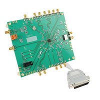
Manufacturer Part Number
LMK04000BEVAL/NOPB
Description
BOARD EVAL PRECISION CLOCK PLL
Manufacturer
National Semiconductor
Series
PowerWise®r
Datasheets
1.LMK04010BISQENOPB.pdf
(54 pages)
2.LMK04002BEVAL.pdf
(56 pages)
3.LMK04002BEVAL.pdf
(38 pages)
Specifications of LMK04000BEVAL/NOPB
Main Purpose
Timing, Clock Conditioner
Embedded
No
Utilized Ic / Part
LMK04000
Primary Attributes
122.88 MHz VCXO
Secondary Attributes
Integrated PLL & VCO
Lead Free Status / RoHS Status
Lead free / RoHS Compliant
Other names
LMK04000BEVAL
LMK04000BEVAL
LMK04000BEVAL


Appendix H: LMK04000
The block diagram in Figure 27 illustrates the functional architecture of the LMK040xxB clock
conditioner. It features a cascaded, dual PLL arrangement, available internal loop filter
components for PLL2, internal VCO with PLL2 for frequency synthesis, and clock distribution
section with individual clock output dividers and delay adjustment blocks. The dual reference
clock input to PLL1 provides fail-safe redundancy for phase locked loop operation. The cascaded
PLL architecture allows PLL1 to be used as a jitter cleaner for an incoming reference clock that
contains excessive phase noise. This requires the user to select an external oscillator (VCXO or
crystal) that provides the desired phase noise performance at the clock output. This external
oscillator becomes the reference clock for PLL2 and along with the phase noise characteristics of
PLL2 and the internal VCO, determines the final phase noise performance at FOUT and the
output of the clock distribution section.
Figure 27 - Functional Block Diagram of the LMK040xxB Dual PLL Precision Clock Conditioner with
CLKin0
CLKin1
DATA
CLK
LE
Interface
uWire
L M K 0 4 0 X X - R E V 3
R
1
PLL1
vcxo
N
1
E V A L U A T I O N
External VCXO module.
R
2
PLL2
50
N
B O A R D
2
CHAN
CHAN
DIV
DIV
VCO
DIV
O P E R A T I N G
LVPECL, LVDS,
5 Output Clock
VCO
Channels
LVCMOS
I N S T R U C T I O N S
CLKout_0
CLKout_4
F
OUT
Related parts for LMK04000BEVAL/NOPB
Image
Part Number
Description
Manufacturer
Datasheet
Request
R

Part Number:
Description:
Low-noise Clock Jitter Cleaner With Cascaded Plls
Manufacturer:
National Semiconductor Corporation
Datasheet:
Part Number:
Description:
Lmk04000 Family Of Precision Clock Conditioners Low-noise Clock Jitter Cleaner With Cascaded Plls
Manufacturer:
National Semiconductor Corporation
Datasheet:

Part Number:
Description:
National Semiconductor [8-Bit D/A Converter]
Manufacturer:
National Semiconductor
Datasheet:
Part Number:
Description:
National Semiconductor [Media Coprocessor]
Manufacturer:
National Semiconductor
Datasheet:
Part Number:
Description:
Digitally Controlled Tone and Volume Circuit with Stereo Audio Power Amplifier, Microphone Preamp Stage and National 3D Sound
Manufacturer:
National Semiconductor
Datasheet:
Part Number:
Description:
Digitally Controlled Tone and Volume Circuit with Stereo Audio Power Amplifier, Microphone Preamp Stage and National 3D Sound
Manufacturer:
National Semiconductor
Datasheet:
Part Number:
Description:
AC97 Rev 2 Codec with Sample Rate Conversion and National 3D Sound
Manufacturer:
National Semiconductor
Part Number:
Description:
Manufacturer:
National Semiconductor
Datasheet:
Part Number:
Description:
Manufacturer:
National Semiconductor
Datasheet:
Part Number:
Description:
General Purpose, Low Voltage, Low Power, Rail-to-Rail Output Operational Amplifiers
Manufacturer:
National Semiconductor
Datasheet:
Part Number:
Description:
8-bit 20 MSPS flash A/D converter.
Manufacturer:
National Semiconductor
Datasheet:
Part Number:
Description:
Low Noise Quad Operational Amplifier
Manufacturer:
National Semiconductor
Datasheet:
Part Number:
Description:
Quad Differential Line Receivers
Manufacturer:
National Semiconductor
Datasheet:
Part Number:
Description:
Quad High Speed Trapezoidal? Bus Transceiver
Manufacturer:
National Semiconductor
Datasheet: