DK-DEV-5M570ZN Altera, DK-DEV-5M570ZN Datasheet - Page 2
DK-DEV-5M570ZN
Manufacturer Part Number
DK-DEV-5M570ZN
Description
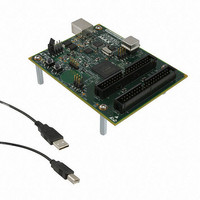
KIT DEV MAX V 5M570Z
Manufacturer
Altera
Series
MAX® Vr
Type
CPLDr
Datasheets
1.DK-DEV-5M570ZN.pdf
(30 pages)
2.DK-DEV-5M570ZN.pdf
(2 pages)
3.DK-DEV-5M570ZN.pdf
(30 pages)
4.DK-DEV-5M570ZN.pdf
(164 pages)
5.DK-DEV-5M570ZN.pdf
(24 pages)
Specifications of DK-DEV-5M570ZN
Contents
Board, Cable(s), Software and Documentation
Silicon Manufacturer
Altera
Core Architecture
CPLD
Core Sub-architecture
MAX
Silicon Core Number
5M
Silicon Family Name
MAX V
Kit Contents
MAX V CPLD Development Board, USB Cable
Rohs Compliant
Yes
Lead Free Status / RoHS Status
Lead free / RoHS Compliant
For Use With/related Products
5M570ZF256
Lead Free Status / Rohs Status
Compliant
Other names
544-2722
Available stocks
Company
Part Number
Manufacturer
Quantity
Price


3–2
Table 3–2. Recommended Operating Conditions for MAX V Devices
Table 3–3. Programming/Erasure Specifications for MAX V Devices
MAX V Device Handbook
V
V
V
V
T
Notes to
(1) MAX V device ISP and/or user flash memory (UFM) programming using JTAG or logic array is not guaranteed outside the recommended
(2) The minimum DC input is –0.5 V. During transitions, the inputs may undershoot to –2.0 V for input currents less than 100 mA and periods
(3) During transitions, the inputs may overshoot to the voltages shown below based on the input duty cycle. The DC case is equivalent to 100%
(4) All pins, including the clock, I/O, and JTAG pins, may be driven before V
Erase and reprogram cycles
Note to
(1) This value applies to the commercial grade devices. For the industrial grade devices, the value is 100 cycles.
J
CCINT
CCIO
I
O
Symbol
operating conditions (for example, if brown-out occurs in the system during a potential write/program sequence to the UFM, Altera recommends
that you read back the UFM contents and verify it against the intended write data).
shorter than 20 ns.
duty cycle. For more information about 5.0-V tolerance, refer to the
V
4.0 V
4.1 V
4.2 V
4.3 V
4.4 V
4.5 V
IN
(1)
(1)
Table
Table
Recommended Operating Conditions
Programming/Erasure Specifications
Parameter
Max. Duty Cycle
100% (DC)
90%
50%
30%
17%
10%
3–3:
1.8-V supply voltage for internal logic and
in-system programming (ISP)
Supply voltage for I/O buffers, 3.3-V
operation
Supply voltage for I/O buffers, 2.5-V
operation
Supply voltage for I/O buffers, 1.8-V
operation
Supply voltage for I/O buffers, 1.5-V
operation
Supply voltage for I/O buffers, 1.2-V
operation
Input voltage
Output voltage
Operating junction temperature
3–2:
Table 3–2
Table 3–3
Parameter
UFM
Configuration flash memory (CFM)
lists recommended operating conditions for the MAX V device family.
lists the programming/erasure specifications for the MAX V device family.
Block
Commercial range
Industrial range
Using MAX V Devices in Multi-Voltage Systems
CCINT
MAX V devices
(2), (3),
Conditions
Chapter 3: DC and Switching Characteristics for MAX V Devices
and V
Minimum
—
—
—
—
—
—
CCIO
—
—
(4)
are powered.
Typical
Minimum
—
—
2.375
1.425
1.71
3.00
1.71
1.14
–0.5
–40
0
0
January 2011 Altera Corporation
Maximum
1000
chapter.
100
Maximum
(1)
2.625
1.575
Operating Conditions
V
1.89
3.60
1.89
1.26
100
4.0
85
CCIO
Cycles
Cycles
Unit
Unit
°C
°C
V
V
V
V
V
V
V
V
Related parts for DK-DEV-5M570ZN
Image
Part Number
Description
Manufacturer
Datasheet
Request
R

Part Number:
Description:
KIT DEV ARRIA II GX FPGA 2AGX125
Manufacturer:
Altera
Datasheet:

Part Number:
Description:
KIT DEV CYCLONE III LS EP3CLS200
Manufacturer:
Altera
Datasheet:

Part Number:
Description:
KIT DEV STRATIX IV FPGA 4SE530
Manufacturer:
Altera
Datasheet:

Part Number:
Description:
KIT DEV FPGA 2AGX260 W/6.375G TX
Manufacturer:
Altera
Datasheet:

Part Number:
Description:
KIT DEV STRATIX V FPGA 5SGXEA7
Manufacturer:
Altera
Datasheet:

Part Number:
Description:
KIT DEVELOPMENT STRATIX III
Manufacturer:
Altera
Datasheet:

Part Number:
Description:
KIT DEVELOPMENT STRATIX IV
Manufacturer:
Altera
Datasheet:

Part Number:
Description:
KIT DEV ARRIA GX 1AGX60N
Manufacturer:
Altera
Datasheet:
Part Number:
Description:
KIT STARTER CYCLONE IV GX
Manufacturer:
Altera
Datasheet:
Part Number:
Description:
KIT DEVELOPMENT STRATIX IV
Manufacturer:
Altera
Datasheet:

Part Number:
Description:
CPLD, EP610 Family, ECMOS Process, 300 Gates, 16 Macro Cells, 16 Reg., 16 User I/Os, 5V Supply, 35 Speed Grade, 24DIP
Manufacturer:
Altera Corporation
Datasheet:
Part Number:
Description:
CPLD, EP610 Family, ECMOS Process, 300 Gates, 16 Macro Cells, 16 Reg., 16 User I/Os, 5V Supply, 15 Speed Grade, 24DIP
Manufacturer:
Altera Corporation
Datasheet: