DK-DEV-5M570ZN Altera, DK-DEV-5M570ZN Datasheet - Page 22
DK-DEV-5M570ZN
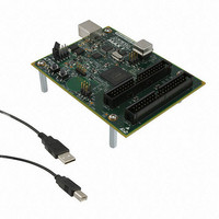
Manufacturer Part Number
DK-DEV-5M570ZN
Description
KIT DEV MAX V 5M570Z
Manufacturer
Altera
Series
MAX® Vr
Type
CPLDr
Datasheets
1.DK-DEV-5M570ZN.pdf
(30 pages)
2.DK-DEV-5M570ZN.pdf
(2 pages)
3.DK-DEV-5M570ZN.pdf
(30 pages)
4.DK-DEV-5M570ZN.pdf
(164 pages)
5.DK-DEV-5M570ZN.pdf
(24 pages)
Specifications of DK-DEV-5M570ZN
Contents
Board, Cable(s), Software and Documentation
Silicon Manufacturer
Altera
Core Architecture
CPLD
Core Sub-architecture
MAX
Silicon Core Number
5M
Silicon Family Name
MAX V
Kit Contents
MAX V CPLD Development Board, USB Cable
Rohs Compliant
Yes
Lead Free Status / RoHS Status
Lead free / RoHS Compliant
For Use With/related Products
5M570ZF256
Lead Free Status / Rohs Status
Compliant
Other names
544-2722
Available stocks
Company
Part Number
Manufacturer
Quantity
Price


3–22
Table 3–31. Global Clock External I/O Timing Parameters for the 5M2210Z Device
Table 3–32. External Timing Input Delay Adders for MAX V Devices (Part 1 of 2)
MAX V Device Handbook
t
t
t
t
f
Note to
(1) The maximum frequency is limited by the I/O standard on the clock input pin. The 16-bit counter critical delay performs faster than this global
3.3-V LVTTL
3.3-V LVCMOS
2.5-V LVTTL /
LVCMOS
1.8-V LVTTL /
LVCMOS
1.5-V LVCMOS
CO
CH
CL
CNT
CNT
Symbol
clock input pin maximum frequency.
Table
External Timing I/O Delay Adders
I/O Standard
Global clock to output delay
Global clock high time
Global clock low time
Minimum global clock period for 16-bit
counter
Maximum global clock frequency for 16-bit
counter
3–31:
Without Schmitt
Trigger
With Schmitt
Trigger
Without Schmitt
Trigger
With Schmitt
Trigger
Without Schmitt
Trigger
With Schmitt
Trigger
Without Schmitt
Trigger
Without Schmitt
Trigger
The I/O delay timing parameters for the I/O standard input and output adders and
the input delays are specified by speed grade, independent of device density.
Table 3–32
pins for all packages. If you select an I/O standard other than 3.3-V LVTTL, add the
input delay adder to the external t
page 3–19
with 16 mA drive strength and fast slew rate, add the output delay adder to the
external t
Parameter
CO
through
through
and t
Min
—
—
—
—
—
—
—
—
5M40Z/ 5M80Z/ 5M160Z/
PD
C4
Table
Table 3–36 on page 3–25
listed in
5M240Z/ 5M570Z
Max
387
387
429
378
681
42
0
0
3–31. If you select an I/O standard other than 3.3-V LVTTL
Table 3–26 on page 3–19
Min
—
—
—
—
—
—
—
—
Condition
10 pF
C5, I5
SU
—
—
—
—
timing parameters listed in
Chapter 3: DC and Switching Characteristics for MAX V Devices
Max
442
442
483
368
658
42
0
0
list the adder delays associated with I/O
Min
216
216
2.0
4.0
—
Min
—
—
—
—
—
—
—
—
C4
(Note 1)
C4
247.5
through
Max
5M1270Z/ 5M2210Z
6.0
—
—
—
1,334
Max
480
480
246
787
695
0
0
(Part 2 of 2)
January 2011 Altera Corporation
Table
Timing Model and Specifications
Min
266
266
2.0
5.0
—
Table 3–26 on
Min
—
—
—
—
—
—
—
—
C5, I5
3–31.
C5, I5
201.1
Max
7.4
1,642
—
—
—
Max
591
591
303
968
855
0
0
MHz
Unit
Unit
ns
ps
ps
ns
ps
ps
ps
ps
ps
ps
ps
ps
Related parts for DK-DEV-5M570ZN
Image
Part Number
Description
Manufacturer
Datasheet
Request
R

Part Number:
Description:
KIT DEV ARRIA II GX FPGA 2AGX125
Manufacturer:
Altera
Datasheet:

Part Number:
Description:
KIT DEV CYCLONE III LS EP3CLS200
Manufacturer:
Altera
Datasheet:

Part Number:
Description:
KIT DEV STRATIX IV FPGA 4SE530
Manufacturer:
Altera
Datasheet:

Part Number:
Description:
KIT DEV FPGA 2AGX260 W/6.375G TX
Manufacturer:
Altera
Datasheet:

Part Number:
Description:
KIT DEV STRATIX V FPGA 5SGXEA7
Manufacturer:
Altera
Datasheet:

Part Number:
Description:
KIT DEVELOPMENT STRATIX III
Manufacturer:
Altera
Datasheet:

Part Number:
Description:
KIT DEVELOPMENT STRATIX IV
Manufacturer:
Altera
Datasheet:

Part Number:
Description:
KIT DEV ARRIA GX 1AGX60N
Manufacturer:
Altera
Datasheet:
Part Number:
Description:
KIT STARTER CYCLONE IV GX
Manufacturer:
Altera
Datasheet:
Part Number:
Description:
KIT DEVELOPMENT STRATIX IV
Manufacturer:
Altera
Datasheet:

Part Number:
Description:
CPLD, EP610 Family, ECMOS Process, 300 Gates, 16 Macro Cells, 16 Reg., 16 User I/Os, 5V Supply, 35 Speed Grade, 24DIP
Manufacturer:
Altera Corporation
Datasheet:
Part Number:
Description:
CPLD, EP610 Family, ECMOS Process, 300 Gates, 16 Macro Cells, 16 Reg., 16 User I/Os, 5V Supply, 15 Speed Grade, 24DIP
Manufacturer:
Altera Corporation
Datasheet: