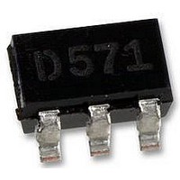
SI3812DV-T1-GE3 Vishay, SI3812DV-T1-GE3 Datasheet

SI3812DV-T1-GE3
Specifications of SI3812DV-T1-GE3
Available stocks
Related parts for SI3812DV-T1-GE3
SI3812DV-T1-GE3 Summary of contents
Page 1
... 2.85 mm Ordering Information: Si3812DV-T1-GE3 (Lead (Pb)-free and Halogen-free) ABSOLUTE MAXIMUM RATINGS (T Parameter Drain-Source Voltage (MOSFET) Reverse Voltage (Schottky) Gate-Source Voltage (MOSFET) Continuous Drain Current (T = 150 °C) (MOSFET) J Pulsed Drain Current (MOSFET) Continuous Source Current (MOSFET Diode Conduction) Average Foward Current (Schottky) ...
Page 2
... Si3812DV Vishay Siliconix THERMAL RESISTANCE RATINGS Parameter a Junction-to-Ambient Junction to Foot (MOSFET Drain, Schottky Cathode) Note: a. Surface mounted on 1" x 1" FR4 board. MOSFET AND SCHOTTKY SPECIFICATIONS (T Parameter Symbol Static V Gate Threshold Voltage Gate-Body Leakage Zero Gate Voltage Drain Current (MOSFET and Schottky) ...
Page 3
... 1.8 1.6 1.4 1.2 1.0 0.8 0.6 2.0 2.5 This document is subject to change without notice. Si3812DV Vishay Siliconix ° °C 125 °C 0.0 0.5 1.0 1.5 2.0 2.5 3.0 3 Gate-to-Source Voltage (V) GS Transfer Characteristics C iss C oss ...
Page 4
... Si3812DV Vishay Siliconix MOSFET TYPICAL CHARACTERISTICS (25 °C, unless otherwise noted 150 ° 0.1 0 0.3 0.6 0 Source-to-Drain Voltage (V) SD Source-Drain Diode Forward Voltage 0 250 µA D 0.2 0.0 - 0.2 - 0 Temperature (°C) J Threshold Voltage 2 1 Duty Cycle = 0.5 0.2 0.1 0.1 0.05 0.02 Single Pulse 0 ...
Page 5
... Normalized Thermal Transient Impedance, Junction-to-Foot 5 1 0.1 100 125 150 150 120 Reverse Voltage (V) KA Capacitance This document is subject to change without notice. Si3812DV Vishay Siliconix 150 ° ° 0.2 0.4 0.6 0 Forward Voltage Drop (V) F Forward Voltage Drop 16 20 www.vishay.com www.vishay.com/doc?91000 10 1 ...
Page 6
... Si3812DV Vishay Siliconix SCHOTTKY TYPICAL CHARACTERISTICS (25 °C, unless otherwise noted Duty Cycle = 0.5 0.2 0.1 0.1 0.05 0.02 Single Pulse 0. Normalized Thermal Transient Impedance, Junction-to-Ambient 2 1 Duty Cycle = 0.5 0.2 0.1 0.1 0.05 0.02 Single Pulse 0. Vishay Siliconix maintains worldwide manufacturing capability. Products may be manufactured at one of several qualified locations. Reliability data for Silicon Technology and Package Reliability represent a composite of all qualified locations ...
Page 7
... Vishay product could result in personal injury or death. Customers using or selling Vishay products not expressly indicated for use in such applications their own risk and agree to fully indemnify and hold Vishay and its distributors harmless from and against any and all claims, liabilities, expenses and damages arising or resulting in connection with such use or sale, including attorneys fees, even if such claim alleges that Vishay or its distributor was negligent regarding the design or manufacture of the part ...


