EVAL-ADF7012DBZ5 Analog Devices Inc, EVAL-ADF7012DBZ5 Datasheet - Page 6
EVAL-ADF7012DBZ5
Manufacturer Part Number
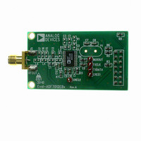
EVAL-ADF7012DBZ5
Description
BOARD DAUGHTER FOR ADF7012
Manufacturer
Analog Devices Inc
Type
Transmitterr
Datasheet
1.EVAL-ADF7012EB1.pdf
(28 pages)
Specifications of EVAL-ADF7012DBZ5
For Use With/related Products
ADF7012
Lead Free Status / RoHS Status
Lead free / RoHS Compliant


ADF7012
ABSOLUTE MAXIMUM RATINGS
T
Table 3.
Parameter
DV
(GND = AGND = DGND = 0 V)
Digital I/O Voltage to GND
Analog I/O Voltage to GND
Operating Temperature Range
TSSOP θ
Lead Temperature, Soldering
Stresses above those listed under Absolute Maximum Ratings
may cause permanent damage to the device. This is a stress
rating only; functional operation of the device at these or any
other conditions above those listed in the operational sections
of this specification is not implied. Exposure to absolute
maximum rating conditions for extended periods may affect
device reliability.
A
Maximum Junction Temperature
Vapor Phase (60 sec)
Infrared (15 sec)
DD
= 25°C, unless otherwise noted.
to GND
JA
Thermal Impedance
Rating
−0.3 V to +3.9 V
−0.3 V to DV
−0.3 V to DV
−40°C to +85°C
150°C
150.4°C/W
215°C
220°C
DD
DD
+ 0.3 V
+ 0.3 V
Rev. A | Page 6 of 28
This device is a high performance RF integrated circuit with an
ESD rating of 1 kV and it is ESD sensitive. Proper precautions
should be taken for handling and assembly.
TRANSISTOR COUNT
35819 (CMOS)
ESD CAUTION
Related parts for EVAL-ADF7012DBZ5
Image
Part Number
Description
Manufacturer
Datasheet
Request
R

Part Number:
Description:
IC, ADJ LDO REG, 1.5V TO 5V 250mA MSOP-8
Manufacturer:
Vishay
Datasheet:

Part Number:
Description:
IC, ADJ LDO REG, 1.5V TO 5V 0.6A 8-TSSOP
Manufacturer:
Vishay
Datasheet:
Part Number:
Description:
IC, ADJ LDO REG, 1.5V TO 5V 250mA MSOP-8
Manufacturer:
Vishay
Datasheet:

Part Number:
Description:
IC ADJ LDO REG 1.5V TO 5V 150mA 5-SOT-23
Manufacturer:
Vishay
Datasheet:

Part Number:
Description:
BOARD EVAL AS1324-AD
Manufacturer:
austriamicrosystems
Datasheet:
Part Number:
Description:
IC, ADJ LDO REG, 1.5V TO 5V 0.6A 8-TSSOP
Manufacturer:
Vishay
Datasheet:

Part Number:
Description:
IC, ADJ LDO REG, 1.5V TO 5V, 0.3A, MSOP8
Manufacturer:
Vishay
Datasheet:
Part Number:
Description:
IC, ADJ LDO REG, 1.5V TO 5V, 0.3A, MSOP8
Manufacturer:
Vishay
Datasheet:
Part Number:
Description:
IC, ADJ LDO REG 1.215V TO 5V 0.3A MSOP-8
Manufacturer:
Vishay
Datasheet:
Part Number:
Description:
IC, ADJ LDO REG 1.215V TO 5V 0.3A MSOP-8
Manufacturer:
Vishay
Datasheet:

Part Number:
Description:
±1.7g Dual-Axis IMEMS Accelerometer Evaluation Board
Manufacturer:
Analog Devices Inc
Datasheet:

Part Number:
Description:
IC MULTIPLIER ANALOG 8-SOIC T/R
Manufacturer:
Analog Devices Inc
Datasheet:

Part Number:
Description:
IC ANALOG MULTIPLIER 8-DIP
Manufacturer:
Analog Devices Inc
Datasheet:
Part Number:
Description:
IC ANALOG MULTIPLIER 8-SOIC
Manufacturer:
Analog Devices Inc
Datasheet:
Part Number:
Description:
IC ANALOG MULTIPLIER 8-DIP
Manufacturer:
Analog Devices Inc
Datasheet: