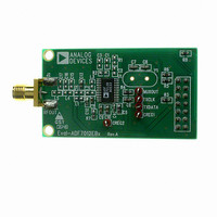
EVAL-ADF7012DBZ5 Analog Devices Inc, EVAL-ADF7012DBZ5 Datasheet - Page 7

EVAL-ADF7012DBZ5
Manufacturer Part Number
EVAL-ADF7012DBZ5
Description
BOARD DAUGHTER FOR ADF7012
Manufacturer
Analog Devices Inc
Type
Transmitterr
Datasheet
1.EVAL-ADF7012EB1.pdf
(28 pages)
Specifications of EVAL-ADF7012DBZ5
For Use With/related Products
ADF7012
Lead Free Status / RoHS Status
Lead free / RoHS Compliant
PIN CONFIGURATION AND FUNCTION DESCRIPTIONS
Table 4. Pin Functional Descriptions
Pin No. Mnemonic
1
2
3
4
5
6
7
8
9
10
11
12
13
14
15
16
17
18
19
20
21
22
23
24
DV
C
CP
TxDATA
TxCLK
MUXOUT
DGND
OSC1
OSC2
CLK
CLK
DATA
LE
CE
L1
L2
C
VCO
RF
RF
DV
AGND
R
C
REG1
VCO
SET
REG2
GND
OUT
OUT
DD
DD
OUT
IN
Description
Positive Supply for the Digital Circuitry. This must be between 2.3 V and 3.6 V. Decoupling capacitors to the analog ground
plane should be placed as close as possible to this pin.
A 1 μF capacitor should be added at C
regulator power-on time, but may cause higher spurious noise.
Charge Pump Output. This output generates current pulses that are integrated in the loop filter. The integrated current
changes the control voltage on the input to the VCO.
Digital data to be transmitted is input on this pin.
GFSK and GOOK Only. This clock output is used to synchronize microcontroller data to the TxDATA pin of the ADF7012. The
clock is provided at the same frequency as the data rate. The microcontroller updates TxDATA on the falling edge of TxCLK.
The rising edge of TxCLK is used to sample TxDATA at the midpoint of each bit.
Provides the Lock_Detect Signal. This signal is used to determine if the PLL is locked to the correct frequency. It also
provides other signals, such as Regulator_Ready, which is an indicator of the status of the serial interface regulator, and a
voltage monitor (see the MUXOUT Modes section for more information).
Ground for Digital Section.
The reference crystal should be connected between this pin and OSC2.
The reference crystal should be connected between this pin and OSC1. A TCXO reference may be used, by driving this pin
with CMOS levels, and powering down the crystal oscillator bit in software.
A divided-down version of the crystal reference with output driver. The digital clock output may be used to drive several
other CMOS inputs, such as a microcontroller clock. The output has a 50:50 mark-space ratio.
Serial Clock Input. This serial clock is used to clock in the serial data to the registers. The data is latched into the
32-bit shift register on the CLK rising edge. This input is a high impedance CMOS input.
Serial Data Input. The serial data is loaded MSB first with the two LSBs being the control bits. This is a high impedance
CMOS input.
Load Enable, CMOS Input. When LE goes high, the data stored in the shift registers is loaded into one of the four latches,
the latch being selected using the control bits.
Chip Enable. Bringing CE low puts the ADF7012 into complete power-down, drawing < 1μA. Register values are lost when
CE is low and the part must be reprogrammed once CE is brought high.
Connected to external printed or discrete inductor. See Choosing the External Inductor Value for advice on the value of the
inductor to be connected between L1 and L2.
Connected to external printed or discrete inductor.
A 22 nF capacitor should be tied between the C
capacitor is necessary to ensure stable VCO operation.
The tuning voltage on this pin determines the output frequency of the voltage controlled oscillator (VCO). The higher the
tuning voltage, the higher the output frequency.
Ground for Output Stage of Transmitter.
The modulated signal is available at this pin. Output power levels are from –16 dBm to +12 dBm. The output should be
impedance matched using suitable components to the desired load. See the PA Matching section.
Voltage supply for VCO and PA section. This should have the same supply as DV
3.6 V. Place decoupling capacitors to the analog ground plane as close as possible to this pin.
Ground Pin for the RF Analog Circuitry.
External Resistor to set charge pump current and some internal bias currents. Use 3.6 kΩ as default.
Add a 470 nF capacitor at C
power-on time and phase noise, but may have stability issues over the supply and temperature.
REG
to reduce regulator noise and improve stability. A reduced capacitor improves regulator
MUXOUT
TxDATA
CLK
CP
TxCLK
C
DGND
OSC1
OSC2
DATA
DV
REG1
Figure 3. Pin Configuration
CLK
REG
OUT
OUT 10
DD
to reduce regulator noise and improve stability. A reduced capacitor improves
Rev. A | Page 7 of 28
11
12
1
2
3
4
5
6
7
8
9
(Not to Scale)
ADF7012
TOP VIEW
TSSOP
VCO
and C
24
23
22
21
20
19
18
17
16
15
14
13
REG2
C
R
AGND
DV
RF
RF
VCO
C
L2
L1
CE
LE
REG2
SET
VCO
DD
OUT
GND
pins. This line should run underneath the ADF7012. This
IN
DD
(Pin 1), and should be between 2.3 V and
ADF7012


