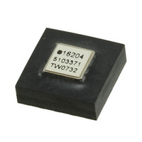
ADIS16204BCCZ Analog Devices Inc, ADIS16204BCCZ Datasheet - Page 13

ADIS16204BCCZ
Manufacturer Part Number
ADIS16204BCCZ
Description
IC ACCEL DIGITAL HI-G 16-LGA
Manufacturer
Analog Devices Inc
Datasheet
1.ADIS16204PCBZ.pdf
(24 pages)
Specifications of ADIS16204BCCZ
Acceleration Range
±37g, 70g
Axis
X, Y
Sensitivity
17.125 LSB/mg, 8.407 LSB/mg
Voltage - Supply
3 V ~ 3.6 V
Output Type
Digital
Bandwidth
400Hz
Interface
SPI
Mounting Type
Surface Mount
Package / Case
16-LGA
No. Of Axes
2
Sensor Case Style
LGA
No. Of Pins
16
Supply Voltage Range
3V To 3.6V
Operating Temperature Range
-40°C To +105°C
Svhc
No SVHC (18-Jun-2010)
Family Name
ADIS16204
Package Type
LGA
Operating Supply Voltage (min)
3V
Operating Supply Voltage (typ)
3.3V
Operating Supply Voltage (max)
3.6V
Operating Temperature (min)
-40C
Operating Temperature (max)
105C
Operating Temperature Classification
Industrial
Product Depth (mm)
8mm
Product Height (mm)
5.2mm
Product Length (mm)
8mm
Mounting
Surface Mount
Pin Count
16
Interface Type
SPI
Sensitivity Per Axis
17.125mg / LSB
Rohs Compliant
Yes
Lead Free Status / RoHS Status
Lead free / RoHS Compliant
For Use With
ADIS16204/PCBZ - BOARD EVAL FOR ADIS16204/PCB
Lead Free Status / Rohs Status
Compliant
Available stocks
Company
Part Number
Manufacturer
Quantity
Price
Company:
Part Number:
ADIS16204BCCZ
Manufacturer:
ST
Quantity:
390
DATA OUTPUT REGISTER ACCESS
Table 6 provides an overview of each data output register,
along with their function, address, and relevant decoding
information.
Sensor Output Data
The ADIS16204 provides access to X- and Y-axis acceleration
measurements, combined accelerations measurements (root
sum square of X and Y), peak acceleration, power supply meas-
urements, temperature measurements, an auxiliary 12-bit
ADC channel, and the event-capture buffer memory.
Peak Sample-and-Hold Output Registers
The ADIS16204 monitors the X, Y and XY acceleration
measurements and holds the maximum value and polarity
for each parameter. The X_PEAK_OUT, Y_PEAK_OUT, and
XY_PEAK_OUT registers provide access to these maximum
values. See the COMMAND register for how to clear these
registers.
Register Access
This output data is continuously updating internally, regardless
of user read rates. The bit map in Table 5 describes the structure of
Table 6. Data Output Register Information
Name
SUPPLY_OUT
XACCL_OUT
YACCL_OUT
AUX_ADC
TEMP_OUT
X_PEAK_OUT
Y_PEAK_OUT
XY_RSS_OUT
XY_PEAK_OUT
CAPT_BUF_1
CAPT_BUF_2
1
2
3
4
25°C, nominal output is equal to 1278 LSB.
The peak levels in these registers accumulate, storing the greatest value measured (polarity is captured—except for XY_PEAK_OUT), until they are cleared using the
COMMAND register.
This is a measure of the total shock absorbed by the package in the XY plane, and is the result of a root sum square of X and Y acceleration measurements.
See the Alarm Detection and Event Capture section for more details.
1
4
4
3
2
2
W/R BIT = 0
SCLK
2, 3
DIN
CS
Function
Power supply
X-axis acceleration
Y-axis acceleration
Auxiliary analog input data
Sensor temperature data
Peak, X-axis acceleration
Peak, Y-axis acceleration
XY combined acceleration (RSS)
Peak, XY combined output (RSS)
Capture Buffer 1 Output Register
Capture Buffer 2 Output Register
ADDRESS = 000101
Figure 23. Example of an Output Timing/Coding Diagram
Rev. B | Page 13 of 24
Register
0x03, 0x02
0x07, 0x06
0x09, 0x08
0x0B, 0x0A
0x0D, 0x0C
0x0F, 0x0E
0x19, 0x18
0x1B, 0x1A
0x1D, 0x1C
0x1F, 0x1E
0x05, 0x04
DOUT
DATA = 1011 1101 1101 1110
NEW DATA, NO ALARM, XACCL_OUT = –9.35025g
all output data registers in the ADIS16204. The upper byte is
always first in register read sequences.
Table 5. Output Bit Assignments
MSB
ND
D7
The MSB holds the new data (ND) indicator. When the output
registers are updated with new data, the ND bit goes to a 1 state.
After the output data is read, it returns to a 0 state. The error/
alarm bit (EA) is used to indicate a system error or an alarm
condition that can result from a number of conditions, such as
a power supply that is out of the specified operating range (see
the Status and Diagnostics section for more details). The output
data is either 12 bits or 14 bits in length. For all of the 12-bit
output data, Bit D13 and Bit D12 are assigned don’t care status.
The output data register map located in Table 6 provides all of
the necessary details for accessing each register’s data. Figure 23
provides an example of the SPI sequence.
Resolution (Bits)
12
14
14
12
12
14
14
14
14
See the Alarm Detection and Event Capture section, Table 37,
and Table 38
EA
D6
D13
D5
Data Format
Binary
Twos complement
Twos complement
Binary
Binary
Twos complement
Twos complement
Binary
Binary
D12
D4
D11
D3
D10
D2
ADIS16204
Scale Factor
(per LSB)
1.22 mV
17.125 mg
8.407 mg
0.61 mV
−0.47°C
17.125 mg
8.407 mg
17.125 mg
17.125 mg
D9
D1
LSB
D8
D0


