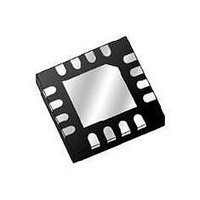
MMA5224WR2 Freescale Semiconductor, MMA5224WR2 Datasheet - Page 10

MMA5224WR2
Manufacturer Part Number
MMA5224WR2
Description
IC ACCELER 240G X-AXIS 16QFN
Manufacturer
Freescale Semiconductor
Datasheet
1.MMA5206WR2.pdf
(63 pages)
Specifications of MMA5224WR2
Sensing Axis
X
Acceleration
240 g
Sensitivity
0.5 g/LSB
Package / Case
QFN-16
Supply Voltage (max)
25 V
Supply Current
4 mA to 8 mA
Maximum Operating Temperature
+ 125 C
Minimum Operating Temperature
- 40 C
Mounting Style
SMD/SMT
Lead Free Status / RoHS Status
Lead free / RoHS Compliant
10
2.8
V
1. Parameters tested 100% at final test.
2. Parameters tested 100% at wafer probe.
3. Verified by characterization
4. * Indicates critical characteristic.
5. Verified by qualification testing.
6. Parameters verified by pass/fail testing in production.
7. Functionality verified 100% via boundary scan. (Timing is directly determined by internal oscillator frequency.)
8. N/A.
9. Verified by simulation.
10. N/A.
11. Measured at V
12. Self-Test repeats on failure up to a ST_RPT
13. N/A.
14. Thermal resistance between the die junction and the exposed pad; cold plate is attached to the exposed pad.
15. Filter cut-off frequencies are directly dependent upon the internal oscillator frequency.
MMA52xxWR
175
176
177
178
179
180
181
182
183
184
185
186
187
188
189
190
191
192
193
194
195
196
197
198
199
200
L
#
≤ (V
Quiescent Current Settling Time (Power Applied to Iq = I
Reset Recovery Internal Delay (After internal POR)
V
V
V
Serial Interface Timing (See
CC
BUF
REG
CC
Survival Time (V
Survival Time (V
Reset Time (V
POR to first Capacitor Test Disconnect
Disconnect Time
Disconnect Delay, Asynchronous Mode
Disconnect Delay, Synchronous Mode
POR to first Capacitor Test Disconnect
Disconnect Time
Disconnect Rate
Clock (SCLK) period (10% of V
Clock (SCLK) high time (90% of V
Clock (SCLK) low time (10% of V
Clock (SCLK) rise time (10% of V
Clock (SCLK) fall time (90% of V
CS asserted to SCLK high (CS = 10% of V
CS asserted to D
Data setup time (D
D
D
SCLK low to data valid (SCLK = 10% of V
SCLK low to CS high (SCLK = 10% of V
CS high to D
CS high to CS low (CS = 90% of V
Dynamic Electrical Characteristics - Supply and SPI
Micro-cut (C
, Capacitor Monitor Disconnect Time
IN
OUT
, V
- V
Data hold time (SCLK = 90% of V
REGA
Data hold time (SCLK = 90% of V
SS
) ≤ V
Capacitor Monitor
CC
OUT
BUF
pin; V
CC
H
CC
CC
=C
OUT
disable (CS = 90% of V
, T
(Figure
disconnect above which Reset is guaranteed)
IN
disconnect without Reset, C
disconnect without Reset, C
REG
SYNC
L
= 10/90% of V
valid (CS = 10% of V
≤ T
=C
Figure
10)
A
REGA
guaranteed across full V
Characteristic
≤ T
CC
=1 μF)
7, C
CC
CC
H
CC
CC
to 10% of V
CC
, ΔT ≤ 25 K/min, unless otherwise specified
CC
to 10% of V
DOUT
to 10% of V
to 90% of V
to 90% of V
CC
to CS = 90% of V
(Figure
to SCLK = 10% of V
(Figure
CC
(Figure
CC
CC
to D
CC
≤ 80 pF, R
CC
CC
to D
to CS = 90% of V
to D
MAX
IN
to D
to SCLK = 10% of V
to D
CC
10)
11)
OUT
CC
= 10/90% of V
BUF
BUF
10)
OUT
CC
CC
)
CC
OUT
times before transmitting Sensor Error Message
OUT
)
)
)
=C
=C
)
= 10/90% of V
DOUT
= Hi Z)
IDLE
= 10/90% of V
REG
REG
= 10/90% of V
CC
IDLE
± 2mA)
)
≥ 10 kΩ)
=C
=C
CC
range.
CC
REGA
REGA
)
CC
)
)
CC
CC
=700 nF)
=1 μF)
CC
)
)
CC
)
)
t
VCC_MICROCUTmin
t
t
t
t
t
t
VCC_MICROCUT
t
t
CAPTEST_ADLY
CAPTEST_SDLY
CAPTEST_RATE
CAPTEST_TIME
CAPTEST_TIME
POR_CAPTEST
POR_CAPTEST
t
VCC_RESET
t
Symbol
HOLD_OUT
t
t
t
t
HOLD_IN
INT_INIT
t
t
ACCESS
t
DISABLE
t
t
t
t
SCLKH
SCLKL
SCLKR
SCLKF
t
SETUP
VALID
t
t
SCLK
LEAD
t
CSN
SET
LAG
1000
Min
320
120
120
30
50
60
20
10
60
⎯
⎯
⎯
⎯
⎯
⎯
⎯
⎯
⎯
⎯
⎯
⎯
⎯
⎯
0
16000 / f
12000 / f
12000 / f
688 / f
256 / f
72 / f
6 / f
6 / f
Typ
15
15
⎯
⎯
⎯
⎯
⎯
⎯
⎯
⎯
⎯
⎯
⎯
⎯
⎯
⎯
⎯
⎯
OSC
OSC
OSC
Freescale Semiconductor
OSC
OSC
OSC
OSC
OSC
Max
1000
40
28
60
50
60
⎯
⎯
⎯
⎯
⎯
⎯
⎯
⎯
⎯
⎯
⎯
⎯
⎯
⎯
⎯
⎯
⎯
⎯
⎯
5
Units
ms
μs
μs
μs
ns
ns
ns
ns
ns
ns
ns
ns
ns
ns
ns
ns
ns
ns
s
s
s
s
s
s
s
s
Sensors
(3)
(7)
(3)
(3)
(3)
(7)
(7)
(7)
(7)
(7)
(7)
(7)
(9)
(9)
(9)
(9)
(9)
(9)
(9)
(9)
(9)
(9)
(9)
(9)
(9)
(9)


