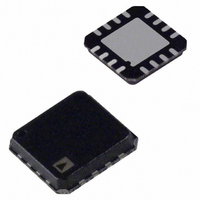
AD8305ACPZ-RL7 Analog Devices Inc, AD8305ACPZ-RL7 Datasheet - Page 19

AD8305ACPZ-RL7
Manufacturer Part Number
AD8305ACPZ-RL7
Description
IC, LOGARITHMIC AMP, 20mV, LFCSP-16
Manufacturer
Analog Devices Inc
Type
Logarithmic Converterr
Datasheet
1.AD8305ACPZ-RL7.pdf
(24 pages)
Specifications of AD8305ACPZ-RL7
No. Of Amplifiers
1
Dynamic Range, Decades
5
Scale Factor V / Decade
0.2
Supply Voltage Range
3V To 12V
Amplifier Case Style
LFCSP
Supply Current
5.4mA
Input Offset Voltage
20mV
Design Resources
Interfacing ADL5315 to Translinear Logarithmic Amplifier (CN0056) Interfacing ADL5317 High Side Current Mirror to a Translinear Logarithmic Amplifier in an Avalanche Photodiode Power Detector
Applications
Fiber Optics
Mounting Type
Surface Mount
Package / Case
16-LFCSP
Rohs Compliant
Yes
Number Of Channels
1
Number Of Elements
3
Power Supply Requirement
Single/Dual
Single Supply Voltage (typ)
5V
Dual Supply Voltage (typ)
±3/±5V
Power Dissipation
500mW
Rail/rail I/o Type
Rail to Rail Output
Single Supply Voltage (min)
3V
Single Supply Voltage (max)
12V
Dual Supply Voltage (min)
±1.5V
Dual Supply Voltage (max)
±6V
Operating Temp Range
-40C to 85C
Operating Temperature Classification
Industrial
Mounting
Surface Mount
Pin Count
16
Package Type
LFCSP EP
Lead Free Status / RoHS Status
Lead free / RoHS Compliant
Lead Free Status / RoHS Status
Lead free / RoHS Compliant, Lead free / RoHS Compliant
Other names
AD8305ACPZ-RL7
CHARACTERIZATION METHODS
During the characterization of the AD8305, the device was
treated as a precision current-input logarithmic converter,
because it is not practical for several reasons to generate
accurate photocurrents by illuminating a photodiode. The test
currents are generated by using well calibrated current sources,
such as the Keithley 236, or by using a high value resistor from a
voltage source to the input pin. Great care is needed when using
very small input currents. For example, the triax output
connection from the current generator was used with the guard
tied to VSUM. The input trace on the PC board was guarded by
connecting adjacent traces to VSUM.
These measures are needed to minimize the risk of leakage
current paths. With 0.5 V as the nominal bias on the INPT pin,
a leakage-path resistance of 1 GΩ to ground would subtract
0.5 nA from the input, which amounts to an error of −0.44 dB
for a source current of 10 nA. Additionally, the very high output
resistance at the input pins and the long cables commonly
needed during characterization allow 60 Hz and RF emissions
to introduce substantial measurement errors. Careful guarding
techniques are essential to reduce the pickup of these spurious
signals.
The primary characterization setup shown in Figure 42 is used
to measure V
conformance, slope and intercept, the voltages appearing at pins
VSUM, INPT and IREF, and the buffer offset and V
temperature. To ensure stable operation over the full current
range of I
C1 = 4.7 nF and R13 = 2 kΩ are used at pin to IREF ground. In
some cases, a fixed resistor between pins VREF and IREF was
used in place of a precision current source. For the dynamic
tests, including noise and bandwidth measurements, more
specialized setups are required.
KEITHLEY 236
KEITHLEY 236
TRIAX CONNECTORS
(SIGNAL – INPT AND IREF
GUARD – VSUM
SHIELD – GROUND)
REF
and temperature extremes, filter components of
REF
Figure 42. Primary Characterization Setup
, the static (dc) performance, logarithmic
IREF
INPT
VREF
CHARACTERIZATION
AD8305
VNEG
DC MATRIX/DC SUPPLIES/DMM
BOARD
VSUM
VPOS
VOUT
VLOG
BFIN
REF
drift with
Rev. B | Page 19 of 24
Figure 43 shows the configuration used to measure the buffer
amplifier bandwidth. The
provisions to offset VLOG at the buffer input, allowing
measurements over the full range of I
The network analyzer input impedances were set to 1 MΩ.
Figure 44. Configuration for Logarithmic Amplifier Bandwidth Measurement
PROVIDES DC OFFSET
Figure 43. Configuration for Buffer Amplifier Bandwidth Measurement
+IN
+IN
EVALUATION
EVALUATION
AD8138
BOARD
AD8138
AD8138
BOARD A
OUTPUT
SPLITTER
OUTPUT
POWER
B
A
B
NETWORK ANALYZER
1nF
INPUT R
NETWORK ANALYZER
1nF
1kΩ
BNC-T
R1
INPUT R
1kΩ
R2
HP 3577A
HP 3577A
1
2
3
4
AD8138
1
2
3
4
INPUT A
IREF
INPT
VRDZ
VREF
INPUT A
VRDZ
IREF
INPT
COMM COMM COMM COMM
VREF
VSUM
COMM COMM COMM COMM
16
VSUM
5
16
5
VNEG VNEG VPOS
evaluation board includes
INPUT B
AD8305
VNEG VNEG VPOS
15
6
INPUT B
AD8305
PD
15
6
using a single supply.
14
7
14
7
13
8
VOUT
SCAL
VLOG
13
BFIN
8
VOUT
SCAL
VLOG
BFIN
0.1µF
0.1µF
AD8305
12
11
10
+V
9
12
11
10
+V
9
S
S


