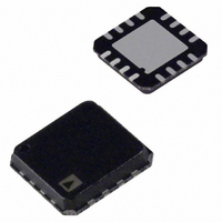
AD8305ACPZ-RL7 Analog Devices Inc, AD8305ACPZ-RL7 Datasheet - Page 5

AD8305ACPZ-RL7
Manufacturer Part Number
AD8305ACPZ-RL7
Description
IC, LOGARITHMIC AMP, 20mV, LFCSP-16
Manufacturer
Analog Devices Inc
Type
Logarithmic Converterr
Datasheet
1.AD8305ACPZ-RL7.pdf
(24 pages)
Specifications of AD8305ACPZ-RL7
No. Of Amplifiers
1
Dynamic Range, Decades
5
Scale Factor V / Decade
0.2
Supply Voltage Range
3V To 12V
Amplifier Case Style
LFCSP
Supply Current
5.4mA
Input Offset Voltage
20mV
Design Resources
Interfacing ADL5315 to Translinear Logarithmic Amplifier (CN0056) Interfacing ADL5317 High Side Current Mirror to a Translinear Logarithmic Amplifier in an Avalanche Photodiode Power Detector
Applications
Fiber Optics
Mounting Type
Surface Mount
Package / Case
16-LFCSP
Rohs Compliant
Yes
Number Of Channels
1
Number Of Elements
3
Power Supply Requirement
Single/Dual
Single Supply Voltage (typ)
5V
Dual Supply Voltage (typ)
±3/±5V
Power Dissipation
500mW
Rail/rail I/o Type
Rail to Rail Output
Single Supply Voltage (min)
3V
Single Supply Voltage (max)
12V
Dual Supply Voltage (min)
±1.5V
Dual Supply Voltage (max)
±6V
Operating Temp Range
-40C to 85C
Operating Temperature Classification
Industrial
Mounting
Surface Mount
Pin Count
16
Package Type
LFCSP EP
Lead Free Status / RoHS Status
Lead free / RoHS Compliant
Lead Free Status / RoHS Status
Lead free / RoHS Compliant, Lead free / RoHS Compliant
Other names
AD8305ACPZ-RL7
PIN CONFIGURATION AND FUNCTION DESCRIPTIONS
Table 3. Pin Function Descriptions
Pin No.
1
2
3
4
5
6, 7
8
9
10
11
12
13 to 16
Mnemonic
VRDZ
VREF
IREF
INPT
VSUM
VNEG
VPOS
VLOG
BFIN
SCAL
VOUT
COMM
EPAD
Function
Top of a Resistive Divider Network that Offsets V
may also be connected to ground when bipolar outputs are to be provided.
Reference Output Voltage of 2.5 V.
Accepts (Sinks) Reference Current, I
Accepts (Sinks) Photodiode Current, I
flows into INPT.
Guard Pin. Used to shield the INPT current line and for optional adjustment of the INPT and I
potential.
Optional Negative Supply, V
Positive Supply, (V
Output of the Logarithmic Front End.
Buffer Amplifier Noninverting Input.
Buffer Amplifier Inverting Input.
Buffer Output.
Analog Ground.
The exposed pad must be soldered to ground.
P
− V
NOTES
1. CONNECT EPAD TO GROUND.
N
VRDZ 1
VREF 2
IREF 3
INPT 4
) ≤ 12 V.
Figure 2. Pin Configuration
N
(this pin is usually grounded; for details of usage, see the Applications section.
Rev. B | Page 5 of 24
(Not to Scale)
AD8305
TOP VIEW
PIN 1
INDICATOR
REF
PD
.
. Usually connected to photodiode anode such that photo current
12 VOUT
11 SCAL
10 BFIN
9 VLOG
LOG
to Position the Intercept. Normally connected to VREF;
REF
node
AD8305


