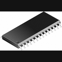
CS8415A-CS Cirrus Logic Inc, CS8415A-CS Datasheet - Page 18

CS8415A-CS
Manufacturer Part Number
CS8415A-CS
Description
IC, DIGITAL AUDIO RECEIVER, SOIC-28
Manufacturer
Cirrus Logic Inc
Specifications of CS8415A-CS
Audio Control Type
Digital
Control Interface
I2C, Serial
Control / Process Application
AV & DVD Receivers, CD-R, Digital Mixing Consoles
Supply Voltage Range
2.85V To 5.5V
Lead Free Status / RoHS Status
Contains lead / RoHS non-compliant
Available stocks
Company
Part Number
Manufacturer
Quantity
Price
Part Number:
CS8415A-CS
Manufacturer:
CIRRUS
Quantity:
20 000
Company:
Part Number:
CS8415A-CSR
Manufacturer:
CirrusLogic
Quantity:
569
Company:
Part Number:
CS8415A-CSZ
Manufacturer:
CIRRUS
Quantity:
108
Part Number:
CS8415A-CSZ
Manufacturer:
CRYSTAL
Quantity:
20 000
CS low, send out the chip address and set the
read/write bit (R/W) high. The next falling edge of
CCLK will clock out the MSB of the addressed
register (CDOUT will leave the high impedance
state). If the MAP auto increment bit is set to 1, the
data for successive registers will appear consecu-
tively.
6.2
In Two-Wire mode, SDA is a bidirectional data
line. Data is clocked into and out of the part by the
clock, SCL, with the clock to data relationship as
shown in Figure 11. There is no CS pin. Each indi-
vidual CS8415A is given a unique address. Pins
AD0 and AD1 form the two least significant bits of
the chip address and should be connected to VL+ or
DGND as desired. The EMPH pin is used to set the
AD2 bit by connecting a resistor from the EMPH
pin to VL+ or to DGND. The state of the pin is
sensed while the CS8415A is being reset. The up-
per 4 bits of the 7-bit address field are fixed at
0010. To communicate with a CS8415A, the chip
address field, which is the first byte sent to the
CS8415A, should match 0010 followed by the set-
tings of the EMPH, AD1, and AD0. The eighth bit
of the address is the R/W bit. If the operation is a
write, the next byte is the Memory Address Pointer
(MAP) which selects the register to be read or writ-
ten. If the operation is a read, the contents of the
18
Two-Wire
Mode
RXP
RXN
RMCK
Power supply pins (VD+, VA+, DGND, AGND) & the reset pin (RST) and the PLL filter pin (FILT)
are om itted from this diagram . Please refer to the Typical Connection Diagram for hook-up details.
AES3 Rx
&
Decoder
RERR
NVERR
Figure 11. Hardware Mode
CHS
COPY ORIG
C & U bit Data Buffer
V L +
H/S
register pointed to by the MAP will be output. Set-
ting the auto increment bit in MAP allows succes-
sive reads or writes of consecutive registers. Each
byte is separated by an acknowledge bit. The ACK
bit is output from the CS8415A after each input
byte is read, and is input to the CS8415A from the
microcontroller after each transmitted byte.The
Two-Wire mode is compatible with the I2C Proto-
col.
6.3
The CS8415A has a comprehensive interrupt capa-
bility. The INT output pin is intended to drive the
interrupt input pin on the host microcontroller. The
INT pin may be set to be active low, active high or
active low with no active pull-up transistor. This
last mode is used for active low, wired-OR hook-
ups, with multiple peripherals connected to the mi-
crocontroller interrupt input pin.
Many conditions can cause an interrupt, as listed in
the interrupt status register descriptions. Each
source may be masked off through mask register
bits. In addition, each source may be set to rising
edge, falling edge, or level sensitive. Combined
with the option of level sensitive or edge sensitive
modes within the microcontroller, many different
configurations are possible, depending on the
needs of the equipment designer.
EMPH
PRO AUDIO
Interrupts
Serial
Audio
Output
RCBL
OLRCK
OSCLK
SDOUT
C
U
CS8415A
DS470PP3


