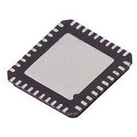
AD9551BCPZ Analog Devices Inc, AD9551BCPZ Datasheet - Page 34

AD9551BCPZ
Manufacturer Part Number
AD9551BCPZ
Description
IC, CLOCK GENERATOR, 806MHZ, LFCSP-40
Manufacturer
Analog Devices Inc
Datasheet
1.AD9551PCBZ.pdf
(40 pages)
Specifications of AD9551BCPZ
Clock Ic Type
Clock Generator
Ic Interface Type
SCI
Frequency
806MHz
No. Of Outputs
2
Supply Current
169mA
Digital Ic Case Style
LFCSP
No. Of Pins
40
Lead Free Status / RoHS Status
Lead free / RoHS Compliant
Available stocks
Company
Part Number
Manufacturer
Quantity
Price
AD9551
Output PLL Control (Register 0x11 to Register 0x19)
Table 26.
Address
0x11
0x12
0x13
0x14
0x15
0x16
0x17
0x18
0x19
Bit
[7:0]
[7:0]
[7:0]
[7:4]
3
2
1
0
[7:0]
[7:0]
[7:4]
3
[2:1]
0
[7:3]
[2:0]
7
6
[5:0]
Bit Name
N
MOD
MOD
MOD
Enable SPI control of
output frequency
Bypass output SDM
Disable output SDM
Reset output PLL
FRAC
FRAC
FRAC
Enable OUTPUT PLL
LOCKED pin as test port
Test mux control
P
P
P
Enable SPI control of
OUT1 dividers
Enable SPI control of
OUT2 divider
P
1
1
0
2
divider
divider
divider
divider
Bits[19:12] of the 20-bit modulus of the output SDM.
Bits[11:4] of the 20-bit modulus of the output SDM.
Bits[3:0] of the 20-bit modulus of the output SDM.
Default is MOD = 1000 0000 0000 0000 0000 (524,288).
Description
8-bit integer divide value for the output SDM. Default is 0x00.
Note that operational limitations impose a lower boundary of 64 (0x40) on N.
Controls output frequency functionality.
0 = output frequency defined by the Y[3:0] pins (default).
1 = contents of Register 0x11 to Register 0x17 define output frequency via N, MOD, and FRAC.
Controls bypassing of the output SDM.
0 = allow integer-plus-fractional division (default).
1 = allow only integer division.
Controls the output SDM internal clocks.
0 = normal operation (SDM clocks active) (default).
1 = SDM disabled (SDM clocks stopped).
Controls initialization of the output PLL.
0 = normal operation (default).
1 = resets the counters and logic associated with the output PLL but does not affect the
output dividers.
Bits[19:12] of the 20-bit fractional part of the output SDM.
Bits[11:4] of the 20-bit fractional part of the output SDM.
Bits[3:0] of the 20-bit fractional part of the output SDM.
Default is FRAC = 0010 0000 0000 0000 0000 (131,072).
Controls functionality of the OUTPUT PLL LOCKED pin (Pin 26).
0 = OUTPUT PLL LOCKED pin indicates status of PLL lock detector (default).
1 = OUTPUT PLL LOCKED pin indicates the signal defined by Bits[2:1].
Selects test mux output.
00 = front end test clock (default).
01 = PFD up divide-by-2.
10 = PFD down divide-by-2.
11 = PLL feedback divide-by-2.
Bit 5 of the 6-bit P
Bits[4:0] of the 6-bit P
P
Bits[2:0] of the 3-bit P
000 = 4 (default).
001 = 5.
010 = 6.
011 = 7.
100 = 8.
101 = 9.
110 = 10.
111 = 11.
The P
Controls functionality of OUT1 dividers.
0 = OUT1 dividers defined by the Y[3:0] pins (default).
1 = contents of Register 0x17 and Register 0x18 define OUT1 dividers (P
Controls functionality of OUT2 divider.
0 = OUT2 divider defined by the Y[3:0] pins (P
1 = contents of Bits[5:0] define P
Bits[5:0] of the 6-bit P
P
These bits are ineffective unless Bit 3 = 1.
1
2
= 100000 (32). The P
= 100000 (32). The P
0
bits are ineffective unless Register 0x19[7] = 1.
Rev. B | Page 34 of 40
1
divider for OUT1.
2
1
divider for OUT2 (1 ≤ P
0
divider for OUT1 (1 ≤ P
2
1
divider for OUT1. The P
bits are ineffective unless Register 0x19[6] = 1.
bits are ineffective unless Register 0x19[7] = 1.
2
.
2
1
≤ 63). Do not set these bits to 000000. Default is
≤ 63). Do not set these bits to 000000. Default is
2
0
= 1) (default).
divide value is as follows:
0
and P
1
).


