AD9551BCPZ Analog Devices Inc, AD9551BCPZ Datasheet - Page 4
AD9551BCPZ
Manufacturer Part Number
AD9551BCPZ
Description
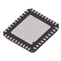
IC, CLOCK GENERATOR, 806MHZ, LFCSP-40
Manufacturer
Analog Devices Inc
Datasheet
1.AD9551PCBZ.pdf
(40 pages)
Specifications of AD9551BCPZ
Clock Ic Type
Clock Generator
Ic Interface Type
SCI
Frequency
806MHz
No. Of Outputs
2
Supply Current
169mA
Digital Ic Case Style
LFCSP
No. Of Pins
40
Lead Free Status / RoHS Status
Lead free / RoHS Compliant
Available stocks
Company
Part Number
Manufacturer
Quantity
Price


AD9551
SPECIFICATIONS
Minimum and maximum values apply for full range of supply voltage and operating temperature variation. Typical values apply for VDD = 3.3 V,
T
REFERENCE CLOCK INPUT CHARACTERISTICS
Table 1.
Parameter
FREQUENCY RANGE
INPUT CAPACITANCE
INPUT RESISTANCE
DUTY CYCLE
REFERENCE CLOCK INPUT VOLTAGE SWING
1
OUTPUT CHARACTERISTICS
Table 2.
Parameter
LVPECL MODE
LVDS MODE
CMOS MODE
The 19 MHz lower limit applies only to the 19.44 MHz operating mode.
A
Differential
Single-Ended
Differential Output Voltage Swing
Common-Mode Output Voltage
Frequency Range
Duty Cycle
Rise/Fall Time
Differential Output Voltage Swing
Offset Voltage
Short-Circuit Output Current
Frequency Range
Duty Cycle
Rise/Fall Time
Output Voltage High, V
Output Voltage Low, V
Frequency Range
= 25°C, unless otherwise noted.
Balanced, V
Unbalanced, ΔV
Common Mode, V
Common-Mode Difference, ΔV
I
I
I
I
OH
OH
OL
OL
= 10 mA
= 1 mA
= 10 mA
= 1 mA
1
1
OD
(20% to 80%)
(20% to 80%)
OD
OS
OL
OH
OS
250
690
VDD − 1.77
247
1.125
Min
19
40
250
Min
0
40
0
40
2.8
2.8
0
1
Typ
3
6
Typ
765
VDD − 1.66
17
255
285
Rev. B | Page 4 of 40
Max
806
60
Max
889
VDD − 1.20
900
60
305
454
25
1.375
25
24
900
60
355
0.5
0.3
200
Unit
MHz
pF
kΩ
%
mV
mV
Unit
mV
V
MHz
%
ps
mV
mV
V
mV
mA
MHz
%
ps
V
V
V
V
MHz
Test Conditions/Comments
Measured single-ended
Measured with a differential probe across
the input pins
Maximum magnitude across pin pair
Peak-to-peak
Test Conditions/Comments
Output driver static
Output driver static
Up to 805 MHz output frequency
100 Ω termination between both pins of
the output driver
Voltage swing between output pins;
output driver static
Absolute difference between voltage
swing of normal pin and inverted pin;
output driver static
Output driver static
Voltage difference between output pins;
output driver static
Up to 805 MHz output frequency
100 Ω termination between both pins of
the output driver
Output driver static; standard drive
strength setting
Output driver static; standard drive
strength setting
3.3 V CMOS; standard drive strength
setting
Related parts for AD9551BCPZ
Image
Part Number
Description
Manufacturer
Datasheet
Request
R

Part Number:
Description:
BOARD EVAL FOR AD9951
Manufacturer:
Analog Devices Inc
Datasheet:


Part Number:
Description:
±1.7g Dual-Axis IMEMS Accelerometer Evaluation Board
Manufacturer:
Analog Devices Inc
Datasheet:

Part Number:
Description:
Inertial Sensor Evaluation System
Manufacturer:
Analog Devices Inc
Datasheet:
Part Number:
Description:
Manufacturer:
Analog Devices Inc
Datasheet:
Part Number:
Description:
Manufacturer:
Analog Devices Inc
Datasheet:
Part Number:
Description:
Manufacturer:
Analog Devices Inc
Datasheet:
Part Number:
Description:
Manufacturer:
Analog Devices Inc
Datasheet:
Part Number:
Description:
Manufacturer:
Analog Devices Inc
Datasheet:
Part Number:
Description:
Manufacturer:
Analog Devices Inc
Datasheet:
Part Number:
Description:
Manufacturer:
Analog Devices Inc
Datasheet:
Part Number:
Description:
Manufacturer:
Analog Devices Inc
Datasheet:
Part Number:
Description:
Manufacturer:
Analog Devices Inc
Datasheet: