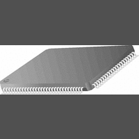
DS90CR483VJD National Semiconductor, DS90CR483VJD Datasheet - Page 3

DS90CR483VJD
Manufacturer Part Number
DS90CR483VJD
Description
IC, LVDS CHANNEL LINK SER/DES, TQFP-100
Manufacturer
National Semiconductor
Datasheet
1.DS90CR483VJD.pdf
(22 pages)
Specifications of DS90CR483VJD
Supply Current
280mA
Supply Voltage Range
3V To 3.6V
Driver Case Style
TQFP
No. Of Pins
100
Operating Temperature Range
-10°C To +70°C
Device Type
Clock
Termination Type
SMD
Filter Terminals
SMD
Rohs Compliant
No
Data Rate Max
5380Mbps
Lead Free Status / RoHS Status
Contains lead / RoHS non-compliant
Available stocks
Company
Part Number
Manufacturer
Quantity
Price
Company:
Part Number:
DS90CR483VJD
Manufacturer:
NS
Quantity:
26
Company:
Part Number:
DS90CR483VJD
Manufacturer:
Texas Instruments
Quantity:
10 000
Company:
Part Number:
DS90CR483VJD/NOPB
Manufacturer:
National Semiconductor
Quantity:
135
Company:
Part Number:
DS90CR483VJD/NOPB
Manufacturer:
Texas Instruments
Quantity:
10 000
Company:
Part Number:
DS90CR483VJDX
Manufacturer:
Texas Instruments
Quantity:
10 000
Company:
Part Number:
DS90CR483VJDX/NOPB
Manufacturer:
Texas Instruments
Quantity:
10 000
CMOS/TTL DC SPECIFICATIONS
V
V
V
V
V
I
I
IN
OS
IH
IL
OH
OL
CL
Absolute Maximum Ratings
If Military/Aerospace specified devices are required,
please contact the National Semiconductor Sales Office/
Distributors for availability and specifications.
Electrical Characteristics
Over recommended operating supply and temperature ranges unless otherwise specified.
Symbol
Supply Voltage (V
CMOS/TTL Input Voltage
LVCMOS/TTL Output
Voltage
LVDS Receiver Input
Voltage
LVDS Driver Output
Voltage
LVDS Output Short
Circuit Duration
Junction Temperature
Storage Temperature
Lead Temperature
(Soldering, 4 sec.)
Maximum Package Power Dissipation Capacity
25˚C
100L TQFP
100 TQFP Package:
DS90CR483VJD
High Level Input
Voltage
Low Level Input
Voltage
High Level Output
Voltage
Low Level Output
Voltage
Input Clamp Voltage
Input Current
Output Short Circuit
Current
Parameter
CC
)
−0.3V to (V
I
I
I
I
V
V
V
OH
OH
OL
CL
−65˚C to +150˚C
IN
IN
OUT
−0.3V to +5.5V
−0.3V to +3.6V
−0.3V to +3.6V
= −18 mA
= 2 mA
= −0.4 mA
= −2mA
= 0.4V, 2.5V or V
= GND
−0.3V to +4V
= 0V
Continuous
CC
(Note 1)
+ 0.3V)
+150˚C
+260˚C
@
2.3W
Conditions
CC
3
Recommended Operating
Conditions
Supply Voltage (V
Operating Free Air
Receiver Input Range
Supply Noise Voltage
Input Clock (TX)
Package Derating:
ESD Rating:
Temperature (T
DS90CR484VJD
DS90CR483VJD
DS90CR484VJD
DS90CR483
(HBM, 1.5kΩ, 100pF)
(EIAJ, 0Ω, 200pF)
DS90CR484
(HBM, 1.5kΩ, 100pF)
(EIAJ, 0Ω, 200pF)
A)
CC
)
GND
Min
−15
2.0
2.7
2.7
18.1mW/˚C above +25˚C
18.1mW/˚C above +25˚C
Min Nom Max
−10
3.0
33
0
−0.79
2.85
+1.8
Typ
3.3
0.1
0
+25
3.3
−120
Max
−1.5
+15
+70
100
112
0.8
0.3
3.6
2.4
www.national.com
>
>
>
>
300 V
200 V
2.3W
6 kV
2 kV
mV
Units
MHz
˚C
V
V
Units
p-p
mA
µA
µA
V
V
V
V
V
V


