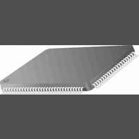
DS90CR483VJD National Semiconductor, DS90CR483VJD Datasheet - Page 5

DS90CR483VJD
Manufacturer Part Number
DS90CR483VJD
Description
IC, LVDS CHANNEL LINK SER/DES, TQFP-100
Manufacturer
National Semiconductor
Datasheet
1.DS90CR483VJD.pdf
(22 pages)
Specifications of DS90CR483VJD
Supply Current
280mA
Supply Voltage Range
3V To 3.6V
Driver Case Style
TQFP
No. Of Pins
100
Operating Temperature Range
-10°C To +70°C
Device Type
Clock
Termination Type
SMD
Filter Terminals
SMD
Rohs Compliant
No
Data Rate Max
5380Mbps
Lead Free Status / RoHS Status
Contains lead / RoHS non-compliant
Available stocks
Company
Part Number
Manufacturer
Quantity
Price
Company:
Part Number:
DS90CR483VJD
Manufacturer:
NS
Quantity:
26
Company:
Part Number:
DS90CR483VJD
Manufacturer:
Texas Instruments
Quantity:
10 000
Company:
Part Number:
DS90CR483VJD/NOPB
Manufacturer:
National Semiconductor
Quantity:
135
Company:
Part Number:
DS90CR483VJD/NOPB
Manufacturer:
Texas Instruments
Quantity:
10 000
Company:
Part Number:
DS90CR483VJDX
Manufacturer:
Texas Instruments
Quantity:
10 000
Company:
Part Number:
DS90CR483VJDX/NOPB
Manufacturer:
Texas Instruments
Quantity:
10 000
LLHT
LHLT
TBIT
TPPOS
TJCC
TCCS
TSTC
THTC
TPDL
TPLLS
TPDD
CLHT
CHLT
RCOP
RCOH
RCOL
RSRC
RHRC
RPDL
RPLLS
RPDD
Symbol
Symbol
Transmitter Switching Characteristics
Over recommended operating supply and temperature ranges unless otherwise specified.
Receiver Switching Characteristics
Over recommended operating supply and temperature ranges unless otherwise specified.
LVDS Low-to-High Transition Time, (Figure 2),
PRE = 0.75V (disabled)
LVDS Low-to-High Transition Time, (Figure 2),
PRE = Vcc (max)
LVDS High-to-Low Transition Time, (Figure 2),
PRE = 0.75V (disabled)
LVDS High-to-Low Transition Time, (Figure 2),
PRE = Vcc (max)
Transmitter Bit Width
Transmitter Pulse Positions -
Normalized
Transmitter Jitter - Cycle-to-Cycle ((Note 8)
TxOUT Channel to Channel Skew
TxIN Setup to TxCLK IN, (Figure 5)
TxIN Hold to TxCLK IN, (Figure 5)
Transmitter Propagation Delay - Latency, (Figure 7)
Transmitter Phase Lock Loop Set, (Figure 9)
Transmitter Powerdown Delay, (Figure 11)
CMOS/TTL Low-to-High Transition Time, (Figure 3),
Rx data out
CMOS/TTL Low-to-High Transition Time, (Figure 3),
Rx clock out
CMOS/TTL High-to-Low Transition Time, (Figure 3),
Rx data out
CMOS/TTL High-to-Low Transition Time, (Figure 3),
Rx clock out
RxCLK OUT Period, (Figure 6)
RxCLK OUT High Time, (Figure 6),
(Note 4)
RxCLK OUT Low Time, (Figure 6),
(Note 4)
RxOUT Setup to RxCLK OUT,
(Figure 6), (Note 4)
RxOUT Hold to RxCLK OUT,
(Figure 6), (Note 4)
Receiver Propagation Delay - Latency, (Figure 8)
Receiver Phase Lock Loop Set, (Figure 10)
Receiver Powerdown Delay, (Figure 12)
Parameter
Parameter
f = 112 MHz
f = 66 MHz
f = 112 MHz
f = 66 MHz
f = 112 MHz
f = 66 MHz
f = 112 MHz
f = 66 MHz
f = 33 to 70
MHz
f = 70 to 112
MHz
5
1.5(TCIP)+3.72
3(TCIP)+4.0
8.928
−250
−200
Min
Min
2.5
3.5
6.0
3.5
6.0
2.4
3.6
3.4
7.0
0
1.5(TCIP)+4.4
3(TCIP)+4.8
1/7 TCIP
0.14
0.11
0.16
0.11
Typ
Typ
50
40
0
0
T
1.5(TCIP)+6.24
3(TCIP)+6.5
+250
+200
Max
100
100
Max
30.3
0.7
0.6
0.8
0.7
10
2.0
1.0
2.0
1.0
10
1
www.national.com
Units
Units
ms
ns
ns
ns
ns
ns
ps
ps
ps
ps
ns
ns
ns
ns
ms
ns
ns
ns
ns
ns
ns
ns
ns
ns
ns
ns
ns
ns
ns
µs


