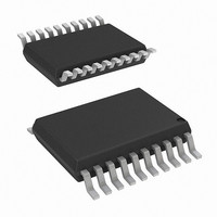
ADUM3470CRSZ Analog Devices Inc, ADUM3470CRSZ Datasheet - Page 25

ADUM3470CRSZ
Manufacturer Part Number
ADUM3470CRSZ
Description
IC, DIGITAL ISOLATOR, 60NS, SSOP-20
Manufacturer
Analog Devices Inc
Series
iCoupler®r
Datasheet
1.EVAL-ADUM3471EBZ.pdf
(32 pages)
Specifications of ADUM3470CRSZ
No. Of Channels
4
Propagation Delay
60ns
Supply Current
33mA
Supply Voltage Range
3V To 3.6V, 4.5V To 5.5V
Digital Ic Case Style
SSOP
No. Of Pins
20
Operating Temperature
-40°C ~ 105°C
Inputs - Side 1/side 2
4/0
Number Of Channels
4
Isolation Rating
2500Vrms
Voltage - Supply
3.3V, 5V
Data Rate
25Mbps
Output Type
Logic
Package / Case
20-SSOP (0.200", 5.30mm Width)
Rohs Compliant
Yes
Lead Free Status / RoHS Status
Lead free / RoHS Compliant
Lead Free Status / RoHS Status
Lead free / RoHS Compliant
APPLICATIONS INFORMATION
THEORY OF OPERATION
The dc-to-dc converter section of the ADuM347x uses a secondary
side controller architecture with isolated pulse-width modulation
(PWM) feedback. V
that switches current to the primary of an external power trans-
former using internal push-pull switches at the X1 and X2 pins.
Power transferred to the secondary side of the transformer is
full-wave rectified with external Schottky diodes (D1 and D2),
filtered with the L1 inductor and C
to the isolated power supply voltage from 3.3 V to 15 V. The
secondary (V
feedback voltage V
creating a PWM control signal that is sent to the primary (V
side by a dedicated iCoupler data channel labeled V
side PWM converter varies the duty cycle of the X1 and X2 switches
to modulate the oscillator circuit and control the power being
sent to the secondary side. This feedback allows for significantly
higher power and efficiency.
The ADuM347x implement undervoltage lockout (UVLO) with
hysteresis on the V
converter does not go into oscillation due to noisy input power or
slow power-on ramp rates.
A minimum load current of 10 mA is recommended to ensure
optimum load regulation. Smaller loads can generate excess noise
on the output due to short or erratic PWM pulses. Excess noise
generated this way can cause regulation problems, in some
circumstances.
APPLICATION SCHEMATICS
The ADuM347x has three main application schematics, as shown
in Figure 38 to Figure 40. Figure 38 has a center-tapped secondary
and two Schottky diodes providing full wave rectification for a
single output, typically for power supplies of 3.3 V, 5 V, 12 V, and
15 V. For single supplies when V
note in Figure 38 about connecting together V
Figure 39 is a voltage doubling circuit that can be used for a single
supply whose output exceeds 15 V, which is the largest supply that
can be connected to the regulator input V
With Figure 39, the output voltage can be as high as 24 V and
the V
doubling secondary circuit, is shown as an example of a coarsely
regulated, positive power supply and an unregulated, negative
power supply, for outputs of approximately ±5 V, ±12 V, and ±15 V.
For any circuit in Figure 38, Figure 39, or Figure 40, the isolated
output voltage (V
and R2 (values 1 kΩ to 100 kΩ), in the application schematics
using the following equation:
where V
approximately 1.25 V.
V
REG
ISO
FB
pin only about 12 V. Figure 40, which also uses a voltage
=
is the internal feedback voltage, which is
V
ISO
FB
) side controller regulates the output by using a
×
ISO
R1
CC
FB
) can be set using the voltage dividers, R1
CC
R2
power input. This feature ensures that the
from a resistor divider on the output and
+
power is supplied to an oscillating circuit
R2
ISO
= 3.3 V or V
OUT
capacitor, and regulated
REG
(Pin 20) of the part.
REG
ISO
, V
= 5 V, see the
ADuM3470/ADuM3471/ADuM3472/ADuM3473/ADuM3474
FB
DD2
. The primary
, and V
ISO
CC
Rev. 0 | Page 25 of 32
.
)
V
V
C
C
CC
CC
IN
V
IN
V
V
CC
C
0.1µF
CC
CC
0.1µF
IN
V
CC
0.1µF
FOR V
Figure 40. Positive and Unregulated Negative Supply
1 X1
2 GND
3 VDD1
4 X2
5 I/OA
6 I/OB
7 I/OC
8 I/OD
9 V
10 GND
1 X1
2 GND
3 V
4 X2
5 I/OA
6 I/OB
7 I/OC
8 I/OD
9 V
10 GND
FOR V
1 X1
2 GND
3 V
4 X2
5 I/OA
6 I/OB
7 I/OC
8 I/OD
9 V
10 GND
DDA
DD1
DDA
ISO
DD1
DDA
1
V
1
1
ISO
1
ISO
= 15V OR LESS, V
1
Figure 39. Doubling Power Supply
1
ADuM3470/
ADuM3471/
ADuM3472/
ADuM3473/
ADuM3474
= V
Figure 38. Single Power Supply
ADuM3470/
ADuM3471/
ADuM3472/
ADuM3473/
ADuM3474
= 3.3V OR 5V CONNECT V
ADuM3470/
ADuM3471/
ADuM3472/
ADuM3473/
ADuM3474
V
FB
ISO
× (R1 + R2)R2
T1
T1
V
= V
ISO
T1
FB
= V
D2
D3
D4
D2
D3
D4
D1
D1
× (R1 + R2)/R2
REG
FB
D1
D2
20 V
19 GND
18 VDD2
17 FB
16 I/OA
15 I/OB
14 I/OC
13 I/OD
12 OC
11 GND
20 V
19 GND
18 V
17 FB
16 I/OA
15 I/OB
14 I/OC
13 I/OD
12 OC
11 GND
× (R1+R2)/R2
CAN CONNECT TO V
20 V
19 GND
18 V
17 FB
16 I/OA
15 I/OB
14 I/OC
13 I/OD
12 OC
11 GND
47µH
47µH
REG
47µH
47µH
REG
DD2
L1
L2
L1
L2
47µH
REG
DD2
C
2
2
2
2
L1
47µF
OUT
REG
2
2
R
, V
R
OC
OC
R
DD2
C
C
47µF
47µF
0.1µF
0.1µF
C
C
OC
47µF
47µF
OUT1
OUT2
100kΩ
100kΩ
0.1µF
OUT1
OUT2
, AND V
+5V
+5V
100kΩ
+5V
ISO
UNREGULATED
.
R1
V
R2
ISO
FB
R1
V
R2
R1
V
R2
+12V TO
.
V
+6V TO
FB
UNREGULATED
FB
TO +15V
+24V
+12V
ISO
REGULATED
V
COARSELY
–5V TO –15V
+5V TO 15V
+3.3V
ISO
V
=
ISO
=
=


