ADSP-BF538BBCZ-5F4 Analog Devices Inc, ADSP-BF538BBCZ-5F4 Datasheet
ADSP-BF538BBCZ-5F4
Specifications of ADSP-BF538BBCZ-5F4


Related parts for ADSP-BF538BBCZ-5F4


ADSP-BF538BBCZ-5F4 Summary of contents
Page 1
... Up to 3.3 V tolerant I/O with specific 5 V tolerant pins 316-ball Pb-free CSP_BGA package MEMORY 148K bytes of on-chip memory: 16K bytes of instruction SRAM/cache 64K bytes of instruction SRAM 32K bytes of data SRAM 32K bytes of data SRAM/cache 4K bytes of scratchpad SRAM 512K 16-bit or 256K 16-bit flash memory (ADSP-BF538F only I0 2. PIO I1 ...
Page 2
... ADSP-BF538/ADSP-BF538F TABLE OF CONTENTS General Description ................................................. 3 Low Power Architecture ......................................... 3 System Integration ................................................ 3 ADSP-BF538/ADSP-BF538F Processor Peripherals ....... 3 Blackfin Processor Core .......................................... 4 Memory Architecture ............................................ 5 DMA Controllers .................................................. 9 Real-Time Clock ................................................... 9 Watchdog Timer ................................................ 10 Timers ............................................................. 10 Serial Ports (SPORTs) .......................................... 10 Serial Peripheral Interface (SPI) Ports ...................... 10 2-Wire Interface ................................................. 11 UART Ports ...................................................... 11 General-Purpose Ports ......................................... 11 Parallel Peripheral Interface ................................... 12 Controller Area Network (CAN) Interface ...
Page 3
... I/O pins. ADSP-BF538/ADSP-BF538F PROCESSOR ADSP- ADSP- PERIPHERALS BF538F4 BF538F8 The ADSP-BF538/ADSP-BF538F processors contain a rich set peripherals connected to the core via several high bandwidth 3 3 buses, providing flexibility in system configuration as well as excellent overall system performance (see the block diagram ...
Page 4
... ADSP-BF538/ADSP-BF538F BLACKFIN PROCESSOR CORE As shown in Figure 2 on Page 4, the Blackfin processor core contains two 16-bit multipliers, two 40-bit accumulators, two 40-bit ALUs, four video ALUs, and a 40-bit shifter. The compu- tation units process 8-bit, 16-bit, or 32-bit data from the register file. ...
Page 5
... C/C++ compiler, resulting in fast and efficient software implementations. MEMORY ARCHITECTURE The ADSP-BF538/ADSP-BF538F processors view memory as a single unified 4G byte address space, using 32-bit addresses. All resources, including internal memory, external memory, and I/O control registers, occupy separate sections of this common address space ...
Page 6
... When connected to AMS3–1 the flash memory appears as non- volatile memory in the processor memory map shown in Figure 3 on Page Flash Memory Programming The ADSP-BF538F4 and ADSP-BF538F8 flash memory may be programmed before or after mounting on the printed circuit board. To program the flash prior to mounting on the printed circuit ...
Page 7
... When an event is triggered, the state of the processors is saved on the supervisor stack. The ADSP-BF538/ADSP-BF538F processors’ event controllers consist of two stages, the core event controller (CEC), and the system interrupt controllers (SIC). The core event controller works with the system interrupt controllers to prioritize and control all system events ...
Page 8
... IVG7 Software Watchdog Timer IVG7 IVG7 Event Control IVG7 The ADSP-BF538/ADSP-BF538F processors provide the user IVG7 with a very flexible mechanism to control the processing of IVG7 events. In the CEC, three registers are used to coordinate and control events. Each register is 32 bits wide: IVG7 • ...
Page 9
... DMA CONTROLLERS The ADSP-BF538/ADSP-BF538F processors have two, inde- pendent DMA controllers that support automated data transfers with minimal overhead for the processor core. DMA transfers can occur between the processor internal memories and any of its DMA capable peripherals ...
Page 10
... CONTACT CRYSTAL MANUFACTURER FOR DETAILS. C1 AND C2 SPECIFICATIONS ASSUME BOARD TRACE CAPACITANCE Figure 5. External Components for RTC WATCHDOG TIMER The ADSP-BF538/ADSP-BF538F processors include a 32-bit timer that can be used to implement a software watchdog func- tion. A software watchdog can improve system availability by forcing the processor to a known state through generation of a ...
Page 11
... The capabilities of the UARTs are further extended with sup- port for the Infrared Data Association (IrDA Physical Layer Link Specification (SIR) protocol. GENERAL-PURPOSE PORTS The ADSP-BF538/ADSP-BF538F processors have gen- eral-purpose I/O pins that are multiplexed with other peripherals. They are arranged into ports and F as shown in Table 4 ...
Page 12
... PPI_CONTROL register. Frame Capture Mode Frame capture mode allows the video source(s) to act as a slave (e.g., for frame capture). The ADSP-BF538/ADSP-BF538F pro- cessors control when to read from the video source(s). PPI_FS1 is an HSYNC output and PPI_FS2 is a VSYNC output. Output Mode Output mode is used for transmitting video or other data with up to three output frame syncs ...
Page 13
... DYNAMIC POWER MANAGEMENT The ADSP-BF538/ADSP-BF538F processors provide four oper- ating modes, each with a different performance/power profile. In addition, dynamic power management provides the control functions to dynamically alter the processor core supply voltage, further reducing power dissipation ...
Page 14
... CAN bus traffic, by asserting the RESET pin external source. Power Savings As shown in Table 6, the ADSP-BF538/ADSP-BF538F proces- sors support three different power domains. The use of multiple power domains maximizes flexibility, while maintaining com- pliance with industry standards and conventions. The 3 ...
Page 15
... Considerations for ADSP-BF533 Blackfin Processor (EE-228) applications note on the Analog Devices website (www.analog.com)—use site search on “EE-228”. CLOCK SIGNALS The ADSP-BF538/ADSP-BF538F processors can be clocked by an external crystal, a sine wave input buffered, shaped clock derived from an external clock oscillator external clock is used, it should be a TTL-compatible signal and must not be halted, changed, or operated below the speci- fied frequency during normal operation ...
Page 16
... ROM memory space is set up using asynchronous memory bank 0. For . Note that SCLK ADSP-BF538F processors, the on-chip flash is booted if FCE is connected to AMS0. All configuration settings are set for the slowest device possible (3-cycle hold time; 15-cycle R/W access times; 4-cycle setup). ...
Page 17
... Code density enhancements, which include intermixing of 16- and 32-bit instructions (no mode switching, no code segregation). Frequently used instructions are encoded in 16 bits. DEVELOPMENT TOOLS The ADSP-BF538/ADSP-BF538F processors are supported with ® † a complete set of CROSSCORE software and hardware devel- opment tools, including Analog Devices emulators and ® ...
Page 18
... File (LDF), allowing the developer to move between the graphi- cal and textual environments. Analog Devices emulators use the IEEE 1149.1 JTAG Test Access Port of the ADSP-BF538/ADSP-BF538F processors to monitor and control the target board processor during emula- tion. The emulator provides full speed emulation, allowing inspection and modification of memory, registers, and proces- sor stacks ...
Page 19
... PIN DESCRIPTIONS The ADSP-BF538/ADSP-BF538F processors pin definitions are listed in Table 10. All pins are three-stated during and immediately after reset, except the memory interface, asynchronous memory control, and synchronous memory control pins, which are driven high active, then the memory pins are also three-stated. All Table 10 ...
Page 20
... ADSP-BF538/ADSP-BF538F Table 10. Pin Descriptions (Continued) Pin Name I/O 2-Wire Interface Port SDA0 I SCL0 I SDA1 I SCL1 I Serial Port0 RSCLK0 I/O RFS0 I/O DR0PRI I DR0SEC I TSCLK0 I/O TFS0 I/O DT0PRI O DT0SEC O Serial Port1 RSCLK1 I/O RFS1 I/O DR1PRI I DR1SEC I TSCLK1 I/O TFS1 I/O ...
Page 21
... GPIO/SPI0 Slave Select Enable 1/Timer Alternate Clock Input GPIO/SPI0 Slave Select Enable 2 GPIO/PPI Frame Sync 3/SPI0 Slave Select Enable 3 GPIO/PPI15/SPI0 Slave Select Enable 4 GPIO/PPI14/SPI0 Slave Select Enable 5 GPIO/PPI13/SPI0 Slave Select Enable 6 GPIO/PPI12/SPI0 Slave Select Enable 7 Rev Page January 2008 ADSP-BF538/ADSP-BF538F Driver Type ...
Page 22
... ADSP-BF538/ADSP-BF538F Table 10. Pin Descriptions (Continued) Pin Name I/O PF8/PPI11 I/O PF9/PPI10 I/O PF10/PPI9 I/O PF11/PPI8 I/O PF12/PPI7 I/O PF13/PPI6 I/O PF14/PPI5 I/O PF15/PPI4 I/O Real-Time Clock RTXI I RTXO O JTAG Port TCK I TDO O TDI I TMS I TRST I EMU O Clock CLKIN I XTAL O Mode Controls ...
Page 23
... AMBIENT The following bidirectional pins are 3.3 V tolerant: DATA15–0, SCK2–0, MISO2–0, MOSI2– The following bi-directional pins are 5 V tolerant: SCL0, SCL1, SDA0, SDA1, CANTX, CANRX, IH Rev Page January 2008 ADSP-BF538/ADSP-BF538F Min Nom Max Unit 0.8 1.25 1 ...
Page 24
... ADSP-BF538/ADSP-BF538F ELECTRICAL CHARACTERISTICS 1 Parameter V High Level Output Voltage OH V Low Level Output Voltage OL I High Level Input Current IH I High Level Input Current JTAG IHP 3 I Low Level Input Current IL I Three-State Leakage Current OZH I Three-State Leakage Current OZL Input Capacitance ...
Page 25
... Rev Page January 2008 ADSP-BF538/ADSP-BF538F Figure 9 and Table 12 provides Ordering Guide on Page 56. a ADSP-BF538 tppZccc vvvvvv.x n.n yyww country_of_origin B Figure 9. Product Information on Package Field Description Temperature Range Package Type RoHS Compliant Part See Ordering Guide Assembly Lot Code ...
Page 26
... Table 13 and Table 14 describe the timing requirements for the ADSP-BF538/ADSP-BF538F processors’ clocks. Take care in selecting MSEL, SSEL, and CSEL ratios so as not to exceed the maximum core clock, system clock, and voltage controlled Table 13. Core Clock (CCLK) Requirements - 400 MHz Models ...
Page 27
... Applies after power-up sequence is complete. At power-up, the processor’s internal phase-locked loop requires no more than 2000 CLKIN cycles, while RESET is asserted, assuming stable power supplies and CLKIN (not including startup time of external clock oscillator). t CKIN CLKIN t CKINL RESET 4 period is 50 ns. CKIN t CKINH t WRST Figure 10. Clock and Reset Timing Rev Page January 2008 ADSP-BF538/ADSP-BF538F Min Max 20.0 100.0 8.0 8 CKIN Unit ...
Page 28
... ADSP-BF538/ADSP-BF538F Asynchronous Memory Read Cycle Timing Table 18 and Table 19 on Page 29 and Figure 11 on Page 29 describe asynchronous memory read cycle opera- tions for synchronous and for asynchronous ARDY. Table 18. Asynchronous Memory Read Cycle Timing with Synchronous ARDY Parameter Timing Requirements t DATA15–0 Setup Before CLKOUT ...
Page 29
... ADDR19–1 AOE ARE t DANR ARDY DATA15–0 Figure 12. Asynchronous Memory Read Cycle Timing with Asynchronous ARDY PROGRAMMED READ ACCESS ACCESS EXTENDED 4 CYCLES BE, ADDRESS t DO Rev Page January 2008 ADSP-BF538/ADSP-BF538F Min Max Unit 2 – 2) × t SCLK 0.0 ns 6.0 ns 0.8 ns HOLD ...
Page 30
... ADSP-BF538/ADSP-BF538F Asynchronous Memory Write Cycle Timing Table 20 and Table 21 on Page 31 and Figure 13 on Page 31 describe asynchronous memory write cycle opera- tions for synchronous and for asynchronous ARDY. Table 20. Asynchronous Memory Write Cycle Timing with Synchronous ARDY Parameter Timing Requirements t ARDY Setup Before the Falling Edge of CLKOUT ...
Page 31
... ARDY t ENDAT DATA15–0 WRITE DATA Figure 14. Asynchronous Memory Write Cycle Timing with Asynchronous ARDY ACCESS PROGRAMMED WRITE EXTENDED ACCESS 2 CYCLES BE, ADDRESS t HO Rev Page January 2008 ADSP-BF538/ADSP-BF538F Min Max ( – 2) × t 0.0 6.0 1.0 6.0 0.8 HOLD 1 CYCLE HAA t DDAT ...
Page 32
... ADSP-BF538/ADSP-BF538F SDRAM Interface Timing Table 22. SDRAM Interface Timing Parameter Timing Requirements t DATA Setup Before CLKOUT SSDAT t DATA Hold After CLKOUT HSDAT Switching Characteristics t CLKOUT Period SCLK t CLKOUT Width High SCLKH t CLKOUT Width Low SCLKL t Command, ADDR, Data Delay After CLKOUT DCAD ...
Page 33
... CLKOUT High to BGH Deasserted Hold Time EBH CLKOUT BR AMSx ADDR19-1 ABE1-0 AWE ARE BG BGH Figure 16. External Port Bus Request and Grant Cycle Timing with Synchronous BR and Figure Rev Page January 2008 ADSP-BF538/ADSP-BF538F Min Max 4.0 0.0 4.5 4.5 3.6 3.6 3.6 3 ...
Page 34
... ADSP-BF538/ADSP-BF538F Table 24. External Port Bus Request and Grant Cycle Timing with Asynchronous BR Parameter Timing Requirement t BR Pulse Width WBR Switching Characteristics t CLKOUT Low to AMSx, Address, and ARE/AWE Disable SD t CLKOUT Low to AMSx, Address, and ARE/AWE Enable SE t CLKOUT High to BG High Setup ...
Page 35
... Figure 21 FRAME DATA0 SYNC IS IS DRIVEN SAMPLED OUT t DFSPE t HOFSPE t t SDRPE HDRPE Figure 18. PPI GP Rx Mode with Internal Frame Sync Timing Rev Page January 2008 ADSP-BF538/ADSP-BF538F Min Max 6.0 15.0 5.0 1.0 2.0 4.0 10.0 0.0 10.0 0.0 Unit ...
Page 36
... ADSP-BF538/ADSP-BF538F DATA0 IS SAMPLED PPI_CLK POLC = 0 PPI_CLK POLC = 1 POLS = 1 PPI_FS1 POLS = 0 POLS = 1 PPI_FS2 POLS = 0 t SDRPE PPI_DATA PPI_CLK POLC = 0 PPI_CLK POLC = 1 POLS = 1 PPI_FS1 POLS = 0 POLS = 1 PPI_FS2 POLS = 0 PPI_DATA FRAME SYNC IS SAMPLED FOR DATA1 IS DATA0 SAMPLED t HFSPE t SFSPE t HDRPE Figure 19. PPI GP Rx Mode with External Frame Sync Timing ...
Page 37
... FRAME SYNC IS REFERENCED TO THIS CLOCK EDGE PPI_CLK POLC = 0 PPI_CLK POLC = 1 t DFSPE t HOFSPE POLS = 1 PPI_FS1 POLS = 0 POLS = 1 PPI_FS2 POLS = 0 PPI_DATA DATA0 IS DRIVEN OUT t DDTPE t HDTPE DATA0 Figure 21. PPI GP Tx Mode with Internal Frame Sync Timing Rev Page January 2008 ADSP-BF538/ADSP-BF538F ...
Page 38
... ADSP-BF538/ADSP-BF538F Serial Port Timing Table 26 through Table 29 on Page 39 and through Figure 23 on Page 40 describe Serial Port operations. Table 26. Serial Ports—External Clock Parameter Timing Requirements t TFSx/RFSx Setup Before TSCLKx/RSCLKx (Externally Generated TFSx/RFSx) SFSE t TFSx/RFSx Hold After TSCLKx/RSCLKx (Externally Generated TFSx/RFSx) ...
Page 39
... HFSI HOFSE RFSx t HDRI DRx DATA TRANSMIT—EXTERNAL CLOCK SAMPLE EDGE TSCLKx t t HFSI HOFSE TFSx DTx Figure 22. Serial Ports Rev Page January 2008 ADSP-BF538/ADSP-BF538F Min Max 1, 2 10.0 0 and t apply. DDTLFSE DTENLFS DRIVE SAMPLE EDGE EDGE t SCLKEW t DFSE t SFSE ...
Page 40
... ADSP-BF538/ADSP-BF538F EXTERNAL RFSx WITH MCE = 1, MFD = 0 RSCLKx RFSx DTx LATE EXTERNAL TFSx TSCLKx TFSx DTx DRIVE SAMPLE DRIVE t t SFSE/I HOFSE/I t DDTTE/I t DTENLFS t DTENE/I 1ST BIT t DDTLFSE DRIVE SAMPLE DRIVE t HOFSE/I t SFSE/I t DDTTE/I t DTENLFS t DTENE/I 1ST BIT t DDTLFSE Figure 23. External Late Frame Sync Rev ...
Page 41
... SPICLM SPICHM t t DDSPIDM HDSPIDM MSB t HSPIDM MSB VALID t DDSPIDM MSB t HSPIDM LSB VALID Figure 24. Serial Peripheral Interface (SPI) Ports—Master Timing Rev Page January 2008 ADSP-BF538/ADSP-BF538F Min Max 7.5 –1.5 2t –1.5 SCLK 2t –1.5 SCLK 2t –1.5 SCLK 4t –1.5 SCLK 2t –1.5 SCLK 2t – ...
Page 42
... ADSP-BF538/ADSP-BF538F Serial Peripheral Interface Ports—Slave Timing Table 31 and Figure 25 describe SPI port’s slave operations. Table 31. Serial Peripheral Interface (SPI) Ports—Slave Timing Parameter Timing Requirements t Serial Clock High Period SPICHS t Serial Clock Low Period SPICLS t Serial Clock Period SPICLK ...
Page 43
... GP Port Pin Input Pulse Width WFI Switching Characteristic t GP Port Pin Output Delay From CLKOUT Low GPOD CLKOUT GPP OUTPUT GPP O/D OUTPUT GPP INPUT t GPOD t GPOD t WFI Figure 26. General-Purpose Port Cycle Timing Rev Page January 2008 ADSP-BF538/ADSP-BF538F Min Max SCLK 0 6 Unit ns ns ...
Page 44
... ADSP-BF538/ADSP-BF538F Timer Cycle Timing Table 33 and Figure 27 describe timer expired operations. The input signal is asynchronous in “width capture mode” and “external clock mode” and has an absolute maximum input fre- quency MHz. SCLK Table 33. Timer Cycle Timing Parameter Timing Characteristics t Timer Pulse Width Input Low ...
Page 45
... System Open-Drain Outputs: CANRX (when configured as PC1) and PC4. TCK TMS TDI TDO SYSTEM INPUTS t SYSTEM OUTPUTS 1 1 3,4 t TCK t t STAP HTAP t DTDO t t SSYS HSYS DSYS Figure 28. JTAG Port Timing Rev Page January 2008 ADSP-BF538/ADSP-BF538F Min Max Unit TCK ns ns ...
Page 46
... ADSP-BF538/ADSP-BF538F OUTPUT DRIVE CURRENTS Figure 29 through Figure 36 on Page 47 voltage characteristics for the output drivers of the ADSP- BF538/ADSP-BF538F processors. The curves represent the cur- rent drive capability of the output drivers as a function of output voltage. 120 100 100 0 0.5 1.0 1.5 SOURCE VOL TAGE (V) Figure 29 ...
Page 47
... V OH –40 –50 – –70 – DDEXT 3.5 4.0 ) DDEXT Rev Page January 2008 ADSP-BF538/ADSP-BF538F V = 2.25V 2.50V 2.75V 0.5 1.0 1.5 2.0 2.5 SOURCE VOLTAGE (V) Figure 37. Drive Current E (Low V ) DDEXT 0.5 1.0 1.5 2.0 2 SOURCE VOLTAGE (V) Figure 38. Drive Current E (High V ...
Page 48
... Example System Hold Time Calculation To determine the data output hold time in a particular system, first calculate the difference between the ADSP-BF538/ADSP-BF538F processor’s output voltage and the input threshold for the device requiring the hold time. C Figure 39 (per data line), and I (per data line) ...
Page 49
... FALL TIME Figure 44. Typical Output Rise and Fall Times (10% to 90%) vs. Load Capaci- 150 200 250 FALL TIME Figure 45. Typical Output Rise and Fall Times (10% to 90%) vs. Load Capaci- 150 200 250 Rev Page January 2008 ADSP-BF538/ADSP-BF538F 12 10 RISE TIME 100 ...
Page 50
... ADSP-BF538/ADSP-BF538F 30 25 RISE TIME 100 LOAD CAPACITANCE (pF) Figure 46. Typical Output Rise and Fall Times (10% to 90%) vs. Load Capacitance for Driver DDEXT RISE TIME 100 LOAD CAPACITANCE (pF) Figure 47. Typical Output Rise and Fall Times (10% to 90%) vs. Load Capacitance for Driver DDEXT FALL TIME ...
Page 51
... JA θ JMA θ JMA θ = 3.6 V (Max) JC Ψ JT Ψ JT Ψ JT × for Rev Page January 2008 ADSP-BF538/ADSP-BF538F are provided for package comparison and printed JA can be used for a first JA by the equation J ( θ × are provided for package comparison and printed ...
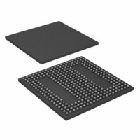
Page 52
... Figure 52. 316-Ball CSP_BGA Ball Configuration (Top View FLASH CONTROL Figure 53. 316-Ball CSP_BGA Ball Configuration (Bottom View) Rev Page January 2008 GND VDDINT VDDRTC NC FLASH CONTROL VDDEXT VROUTx I/O Note: H18 and Y14 are NC for ADSP-BF538 and I/O (FCE and RESET) for ADSP-538F. A1 BALL ...
Page 53
... R18 J8 GND M12 GND R19 J9 GND M13 GND R20 J10 GND M14 VDDINT T1 J11 GND M18 TFS3 T2 Rev Page January 2008 ADSP-BF538/ADSP-BF538F Ball No. Signal M19 ABE0 T3 GND M20 ABE1 T7 VDDEXT W2 N1 TFS0 T8 VDDEXT W3 DR0PRI T9 VDDEXT W4 GND T10 VDDEXT W5 N7 VDDEXT T11 ...
Page 54
... ADSP-BF538/ADSP-BF538F Table 38. 316-Ball CSP_BGA Ball Assignment (Alphabetically by Signal) Signal Ball No. Signal Ball No. Signal Ball No. Signal Ball No. Signal Ball No. Signal ABE0 M19 DATA8 Y6 ABE1 M20 DATA9 W6 ADDR1 N19 DATA10 Y5 ADDR2 N20 DATA11 W5 ADDR3 P19 DATA12 Y4 ADDR4 P20 DATA13 W4 ADDR5 R19 DATA14 Y3 ADDR6 ...
Page 55
... CENTER DIMENSIONS ARE NOMINAL. Figure 54. 316-Ball Chip Scale Package Ball Grid Array [CSP_BGA] (BC-316) 15.20 BSC SQ 0.80 BSC BALL PITCH 0.12 MAX COPLANARITY 0.50 BALL DIAMETER 0.45 0.40 Rev Page January 2008 ADSP-BF538/ADSP-BF538F A1 BALL BOTTOM VIEW 0.30 MIN SEATING PLANE DETAIL A ...
Page 56
... ADSP-BF538BBCZ-4A – +85 C 400 MHz ADSP-BF538BBCZ-5A – +85 C 533 MHz ADSP-BF538BBCZ-4F4 – +85 C 400 MHz ADSP-BF538BBCZ-4F8 – +85 C 400 MHz ADSP-BF538BBCZ-5F4 – +85 C 533 MHz ADSP-BF538BBCZ-5F8 – +85 C 533 MHz RoHS Compliant Part. 2 Referenced temperature is ambient temperature. ©2008 Analog Devices, Inc. All rights reserved. Trademarks and registered trademarks are the property of their respective owners ...