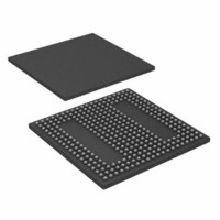
ADSP-BF538BBCZ-5F4 Analog Devices Inc, ADSP-BF538BBCZ-5F4 Datasheet - Page 14

ADSP-BF538BBCZ-5F4
Manufacturer Part Number
ADSP-BF538BBCZ-5F4
Description
IC, FLOAT-PT DSP, 16BIT, 533MHZ, BGA-316
Manufacturer
Analog Devices Inc
Series
Blackfinr
Type
Fixed Pointr
Specifications of ADSP-BF538BBCZ-5F4
No. Of Bits
16 Bit
Frequency
533MHz
Supply Voltage
1.25V
Embedded Interface Type
CAN, I2C, PPI, SPI, TWI, UART
No. Of I/o's
54
Flash Memory Size
512KB
Interface
CAN, SPI, SSP, TWI, UART
Clock Rate
533MHz
Non-volatile Memory
FLASH (512 kB)
On-chip Ram
148kB
Voltage - I/o
3.00V, 3.30V
Voltage - Core
1.25V
Operating Temperature
-40°C ~ 85°C
Mounting Type
Surface Mount
Package / Case
316-CSPBGA
Lead Free Status / RoHS Status
Lead free / RoHS Compliant
For Use With
ADZS-BFAUDIO-EZEXT - BOARD EVAL AUDIO BLACKFIN
Lead Free Status / RoHS Status
Lead free / RoHS Compliant, Lead free / RoHS Compliant
ADSP-BF538/ADSP-BF538F
RTC. When in deep sleep mode, an RTC asynchronous inter-
rupt causes the processor to transition to the active mode.
Assertion of RESET while in deep sleep mode causes the proces-
sor to transition to the full on mode after processor reset.
Hibernate State—Maximum Static Power Savings
The hibernate state maximizes static power savings by disabling
the voltage and clocks to the processor core (CCLK) and to all
the synchronous peripherals (SCLK). The internal voltage regu-
lator for the processor can be shut off by writing b#00 to the
FREQ bits of the VR_CTL register. This disables both CCLK
and SCLK. Furthermore, it sets the internal power supply volt-
age (V
dissipation. Any critical information stored internally (memory
contents, register contents, etc.) must be written to a nonvolatile
storage device prior to removing power if the processor state is
to be preserved. Since V
the external pins three-state, unless otherwise specified. This
allows other devices that may be connected to the processor to
still have power applied without drawing unwanted current.
The internal supply regulator can be woken up either by a real-
time clock wake-up, by CAN bus traffic, by asserting the RESET
pin, or by an external source.
Power Savings
As shown in
sors support three different power domains. The use of multiple
power domains maximizes flexibility, while maintaining com-
pliance with industry standards and conventions. The 3.3 V
V
the RTC can remain functional when the rest of the chip is pow-
ered off. The 1.25 V V
internal logic except for the RTC logic. The 3.3 V V
domain supplies all the I/O except for the RTC crystal. There
are no sequencing requirements for the various power domains.
Table 6. Power Domains
The V
is to operate while the rest of the chip is powered down) or
should be connected to the V
V
nate state, and should also be powered even if the RTC
functionality is not being used in an application.
The power dissipated by a processor is largely a function of the
clock frequency of the processor and the square of the operating
voltage. For example, reducing the clock frequency by 25%
results in a 25% reduction in dynamic power dissipation, while
reducing the voltage by 25% reduces dynamic power dissipation
by more than 40%. Further, these power savings are additive, in
that if the clock frequency and supply voltage are both reduced,
the power savings can be dramatic.
Power Domain
RTC Crystal I/O and Logic
All Internal Logic Except RTC
All I/O Except RTC
DDRTC
DDRTC
DDRTC
DDINT
power domain supplies the RTC I/O and logic so that
should remain powered when the processor is in hiber-
) to 0 V to provide the lowest static power
should either be connected to a battery (if the RTC
Table
6, the ADSP-BF538/ADSP-BF538F proces-
DDINT
DDEXT
power domain supplies all the
DDEXT
is still supplied in this mode, all of
plane on the board. The
V
V
V
V
DDRTC
DDINT
DDEXT
DD
Range
Rev. A | Page 14 of 56 | January 2008
DDEXT
power
100µF
The dynamic power management feature of the processor
allows both the processor’s input voltage (V
quency (f
The savings in power dissipation can be modeled using the
power savings factor and % power savings calculations.
The power savings factor is calculated as
where
f
f
V
V
T
T
The power savings factor is calculated as
VOLTAGE REGULATION
The Blackfin processor provides an on-chip voltage regulator
that can generate processor core voltage levels of 0.8 V
(–5%/+10%) to 1.2 V (–5%/+10%) and 1.25 V (–4% to +10%)
from an external 2.7 V to 3.6 V supply.
cal external components required to complete the power
management system.
CCLKNOM
CCLKRED
NOM
RED
DDINTNOM
DDINTRED
2.25V TO 3.6V
INPUT VOLTAGE
RANGE
NOTE: DESIGNER SHOULD MINIMIZE
TRACE LENGTH TO FDS9431A.
% Power Savings
is the duration running at f
is the duration running at f
+
LOW ESR
is the reduced core clock frequency.
Power Savings Factor
is the nominal core clock frequency.
10µF
CCLK
=
is the reduced internal supply voltage.
is the nominal internal supply voltage.
-------------------- -
f
f
CCLKNOM
CCLKRED
) to be dynamically controlled.
100nF
Figure 6. Voltage Regulator Circuit
(LOW-INDUCTANCE)
FDS9431A
×
=
V
⎛
⎝
(
DDEXT
V
------------------------ -
V
1 Power Savings Factor
DDINTNOM
DDINTRED
–
ZHCS1000
CCLKRED
INDUCTANCE WIRE
SHORT AND LOW-
CCLKNOM
⎞
⎠
10µH
SET OF DECOUPLING
2
×
.
CAPACITORS
Figure 6
100µF
.
⎛
⎝
------------ -
T
100µF
T
NOM
RED
DDINT
+
+
⎞
⎠
shows the typi-
) and clock fre-
) 100%
×
V
V
GND
VR
VR
DDEXT
DDINT
OUT
OUT


