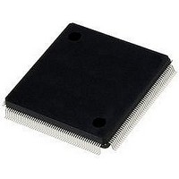
LFE2-20E-5QN208C LATTICE SEMICONDUCTOR, LFE2-20E-5QN208C Datasheet - Page 103

LFE2-20E-5QN208C
Manufacturer Part Number
LFE2-20E-5QN208C
Description
IC, LATTICEECP2 FPGA, 420MHZ, QFP-208
Manufacturer
LATTICE SEMICONDUCTOR
Series
LatticeECP2r
Datasheet
1.LFE2-12E-5FN256C.pdf
(385 pages)
Specifications of LFE2-20E-5QN208C
No. Of Logic Blocks
21000
No. Of Macrocells
10500
No. Of Speed Grades
5
No. Of I/o's
131
Clock Management
DLL, PLL
I/o Supply Voltage
3.465V
Total Ram Bits
276Kbit
Lead Free Status / RoHS Status
Lead free / RoHS Compliant
Available stocks
Company
Part Number
Manufacturer
Quantity
Price
Company:
Part Number:
LFE2-20E-5QN208C
Manufacturer:
Lattice Semiconductor Corporation
Quantity:
10 000
- Current page: 103 of 385
- Download datasheet (3Mb)
Signal Descriptions (Cont.)
Lattice Semiconductor
[LOC]_SQ_VCCOBm
[LOC]_SQ_HDOUTNm
[LOC]_SQ_HDOUTPm
[LOC]_SQ_HDINNm
[LOC]_SQ_HDINPm
[LOC]_SQ_VCCTXm
[LOC]_SQ_VCCRXm
1. These signals are relevant for LatticeECP2M family.
2. m defines the associated channel in the Quad.
3. These signals are defined in Quads [LOC] indicates the corner SERDES Quad is located: ULC (upper left), URC (upper right), LLC (lower
4. When placing switching I/Os around these critical pins that are designed to supply the device with the proper reference or supply voltage,
left), LRC (lower right).
care must be given. For more information, refer to technical note TN1159, LatticeECP2/M Pin Assignment Recommendations.
Signal Name
4
4
I/O
—
—
—
O
O
I
I
Output buffer power supply, channel m (1.2V/1.5V). This pin should be left
floating if the channel is unused.
High-speed output, negative channel m
High-speed output, positive channel m
High-speed input, negative channel m
High-speed input, positive channel m
Transmitter power supply, channel m (1.2V). This pin must be tied to 1.2V
even if the channel is unused.
Receiver power supply, channel m (1.2V). This pin must be tied to 1.2V even if
the channel is unused.
4-3
LatticeECP2/M Family Data Sheet
Description
Pinout Information
Related parts for LFE2-20E-5QN208C
Image
Part Number
Description
Manufacturer
Datasheet
Request
R
Part Number:
Description:
IC, LATTICEECP2 FPGA, 420MHZ, FPBGA-484
Manufacturer:
LATTICE SEMICONDUCTOR
Datasheet:
Part Number:
Description:
IC, LATTICEECP2 FPGA, 420MHZ, FPBGA-672
Manufacturer:
LATTICE SEMICONDUCTOR
Datasheet:

Part Number:
Description:
IC, LATTICEECP2 FPGA, 420MHZ, QFP-208
Manufacturer:
LATTICE SEMICONDUCTOR
Datasheet:
Part Number:
Description:
FPGA LatticeECP2 Family 21000 Cells 90nm (CMOS) Technology 1.2V 256-Pin FBGA
Manufacturer:
LATTICE SEMICONDUCTOR
Datasheet:
Part Number:
Description:
FPGA LatticeECP2 Family 21000 Cells 90nm (CMOS) Technology 1.2V 484-Pin FBGA
Manufacturer:
LATTICE SEMICONDUCTOR
Datasheet:
Part Number:
Description:
FPGA LatticeECP2 Family 21000 Cells 90nm (CMOS) Technology 1.2V 484-Pin FBGA
Manufacturer:
LATTICE SEMICONDUCTOR
Datasheet:
Part Number:
Description:
FPGA LatticeECP2 Family 21000 Cells 90nm (CMOS) Technology 1.2V 484-Pin FBGA
Manufacturer:
LATTICE SEMICONDUCTOR
Datasheet:
Part Number:
Description:
FPGA LatticeECP2 Family 21000 Cells 90nm (CMOS) Technology 1.2V 484-Pin FBGA
Manufacturer:
LATTICE SEMICONDUCTOR
Datasheet:
Part Number:
Description:
FPGA LatticeECP2 Family 21000 Cells 90nm (CMOS) Technology 1.2V 672-Pin FBGA
Manufacturer:
LATTICE SEMICONDUCTOR
Datasheet:
Part Number:
Description:
ISPLSI2032-80LT44Lattice Semiconductor [In-System Programmable High Density PLD]
Manufacturer:
Lattice Semiconductor Corp.
Datasheet:
Part Number:
Description:
IC PROGRAMMED LATTICE GAL 16V8
Manufacturer:
Lattice Semiconductor Corp.
Datasheet:
Part Number:
Description:
357-036-542-201 CARDEDGE 36POS DL .156 BLK LOPRO
Manufacturer:
Lattice Semiconductor Corp.
Datasheet:
Part Number:
Description:
357-036-542-201 CARDEDGE 36POS DL .156 BLK LOPRO
Manufacturer:
Lattice Semiconductor Corp.
Datasheet:
Part Number:
Description:
357-036-542-201 CARDEDGE 36POS DL .156 BLK LOPRO
Manufacturer:
Lattice Semiconductor Corp.
Datasheet:
Part Number:
Description:
357-036-542-201 CARDEDGE 36POS DL .156 BLK LOPRO
Manufacturer:
Lattice Semiconductor Corp.
Datasheet:


