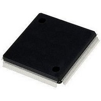
LFE2-20E-5QN208C LATTICE SEMICONDUCTOR, LFE2-20E-5QN208C Datasheet - Page 125

LFE2-20E-5QN208C
Manufacturer Part Number
LFE2-20E-5QN208C
Description
IC, LATTICEECP2 FPGA, 420MHZ, QFP-208
Manufacturer
LATTICE SEMICONDUCTOR
Series
LatticeECP2r
Datasheet
1.LFE2-12E-5FN256C.pdf
(385 pages)
Specifications of LFE2-20E-5QN208C
No. Of Logic Blocks
21000
No. Of Macrocells
10500
No. Of Speed Grades
5
No. Of I/o's
131
Clock Management
DLL, PLL
I/o Supply Voltage
3.465V
Total Ram Bits
276Kbit
Lead Free Status / RoHS Status
Lead free / RoHS Compliant
Available stocks
Company
Part Number
Manufacturer
Quantity
Price
Company:
Part Number:
LFE2-20E-5QN208C
Manufacturer:
Lattice Semiconductor Corporation
Quantity:
10 000
- Current page: 125 of 385
- Download datasheet (3Mb)
Lattice Semiconductor
LFE2-6E/SE and LFE2-12E/SE Logic Signal Connections: 144 TQFP (Cont.)
* Supports true LVDS. Other differential signals must be emulated with external resistors.
** These dedicated input pins can be used for GPLLs or GDLLs within the respective quadrant.
Note: VCCIO and GND pads are used to determine the average DC current drawn by I/Os between GND/VCCIO connections, or between the
last GND/VCCIO in an I/O bank and the end of an I/O bank. The substrate pads listed in the Pin Table do not necessarily have a one-to-one
connection with a package ball or pin.
Number
Pin
136
137
138
139
140
141
142
143
144
Function
Pin/Pad
VCCAUX
VCCIO0
PT6B
PT6A
PT4B
PT4A
PT2B
PT2A
GND
Bank
LFE2-6E/SE
0
0
0
0
0
0
0
-
-
Dual Function
VREF2_0
VREF1_0
Differential
4-25
C
C
C
T
T
T
Function
Pin/Pad
VCCAUX
VCCIO0
PT16B
PT16A
PT6B
PT6A
PT2B
PT2A
GND
LatticeECP2/M Family Data Sheet
Bank
0
0
0
0
0
0
0
-
-
LFE2-12E/12SE
Function
VREF2_0
VREF1_0
Dual
Pinout Information
Differential
C
C
C
T
T
T
Related parts for LFE2-20E-5QN208C
Image
Part Number
Description
Manufacturer
Datasheet
Request
R
Part Number:
Description:
IC, LATTICEECP2 FPGA, 420MHZ, FPBGA-484
Manufacturer:
LATTICE SEMICONDUCTOR
Datasheet:
Part Number:
Description:
IC, LATTICEECP2 FPGA, 420MHZ, FPBGA-672
Manufacturer:
LATTICE SEMICONDUCTOR
Datasheet:

Part Number:
Description:
IC, LATTICEECP2 FPGA, 420MHZ, QFP-208
Manufacturer:
LATTICE SEMICONDUCTOR
Datasheet:
Part Number:
Description:
FPGA LatticeECP2 Family 21000 Cells 90nm (CMOS) Technology 1.2V 256-Pin FBGA
Manufacturer:
LATTICE SEMICONDUCTOR
Datasheet:
Part Number:
Description:
FPGA LatticeECP2 Family 21000 Cells 90nm (CMOS) Technology 1.2V 484-Pin FBGA
Manufacturer:
LATTICE SEMICONDUCTOR
Datasheet:
Part Number:
Description:
FPGA LatticeECP2 Family 21000 Cells 90nm (CMOS) Technology 1.2V 484-Pin FBGA
Manufacturer:
LATTICE SEMICONDUCTOR
Datasheet:
Part Number:
Description:
FPGA LatticeECP2 Family 21000 Cells 90nm (CMOS) Technology 1.2V 484-Pin FBGA
Manufacturer:
LATTICE SEMICONDUCTOR
Datasheet:
Part Number:
Description:
FPGA LatticeECP2 Family 21000 Cells 90nm (CMOS) Technology 1.2V 484-Pin FBGA
Manufacturer:
LATTICE SEMICONDUCTOR
Datasheet:
Part Number:
Description:
FPGA LatticeECP2 Family 21000 Cells 90nm (CMOS) Technology 1.2V 672-Pin FBGA
Manufacturer:
LATTICE SEMICONDUCTOR
Datasheet:
Part Number:
Description:
ISPLSI2032-80LT44Lattice Semiconductor [In-System Programmable High Density PLD]
Manufacturer:
Lattice Semiconductor Corp.
Datasheet:
Part Number:
Description:
IC PROGRAMMED LATTICE GAL 16V8
Manufacturer:
Lattice Semiconductor Corp.
Datasheet:
Part Number:
Description:
357-036-542-201 CARDEDGE 36POS DL .156 BLK LOPRO
Manufacturer:
Lattice Semiconductor Corp.
Datasheet:
Part Number:
Description:
357-036-542-201 CARDEDGE 36POS DL .156 BLK LOPRO
Manufacturer:
Lattice Semiconductor Corp.
Datasheet:
Part Number:
Description:
357-036-542-201 CARDEDGE 36POS DL .156 BLK LOPRO
Manufacturer:
Lattice Semiconductor Corp.
Datasheet:
Part Number:
Description:
357-036-542-201 CARDEDGE 36POS DL .156 BLK LOPRO
Manufacturer:
Lattice Semiconductor Corp.
Datasheet:


