74LV74D NXP Semiconductors, 74LV74D Datasheet - Page 2
74LV74D
Manufacturer Part Number
74LV74D
Description
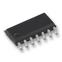
IC, 74LV, SMD, 74LV74, SOIC14, 3.3V
Manufacturer
NXP Semiconductors
Datasheet
1.74LV74D.pdf
(12 pages)
Specifications of 74LV74D
Flip-flop Type
D
Propagation Delay
23ns
Frequency
76MHz
Output Current
12mA
Supply Voltage Range
1V To 5.5V
Logic Case Style
SOIC
No. Of Pins
14
Operating
RoHS Compliant
Trigger Type
Positive Edge
Ic Output Type
Complementary
Rohs Compliant
Yes
Available stocks
Company
Part Number
Manufacturer
Quantity
Price
Company:

Part Number:
74LV74D
Manufacturer:
PHILIPS
Quantity:
4 901
Part Number:
74LV74DB
Manufacturer:
PHILIPS/飞利浦
Quantity:
20 000


1. C
2. The condition is V
Philips Semiconductors
FEATURES
QUICK REFERENCE DATA
GND = 0V; T
NOTES:
ORDERING INFORMATION
PIN DESCRIPTION
t
f
C
C
14-Pin Plastic DIL
14-Pin Plastic SO
14-Pin Plastic SSOP Type II
14-Pin Plastic TSSOP Type I
1, 13
2, 12
3, 11
4, 10
5, 9
6, 8
7
14
1998 Apr 20
PHL
max
Wide operating voltage: 1.0 to 5.5V
Optimized for Low Voltage applications: 1.0 to 3.6V
Accepts TTL input levels between V
Typical V
T
Typical V
T
Output capability: standard
I
Dual D-type flip-flop with set and reset;
positive edge-trigger
I
PD
CC
NUMBER
P
f
f
S (C
amb
amb
i
o
PD
D
= input frequency in MHz; C
SYMBOL
/t
= output frequency in MHz; V
category: flip-flops
PIN
PLH
= C
= 25 C
= 25 C
L
is used to determine the dynamic power dissipation (P
PD
OLP
OHV
V
amb
PACKAGES
CC
(output ground bounce) t 0.8V @ V
(output V
V
2
= 25 C; t
CC
SYMBOL
1CP, 2CP
1R
1S
1Q, 2Q
1D, 2D
1Q
2
GND
f
I
V
D,
D,
Propagation delay
nCP to nQ, nQ
nS
nR
Maximum clock frequency
Input capacitance
Power dissipation capacitance per flip-flop
o
x f
= GND to V
) = sum of the outputs.
,
CC
2R
2S
2Q
D
D
i
OH
r
)S (C
to nQ, nQ
to nQ, nQ
D
D
=t
undershoot) u 2V @ V
f
v2.5 ns
Asynchronous reset-direct input
(active-LOW)
Data inputs
Clock input (LOW-to-HIGH),
edge-triggered)
Asynchronous set-direct input
(active-LOW)
True flip-flop outputs
Complement flip-flop outputs
Ground (0V)
Positive supply voltage
L
L
CC
= output load capacitance in pF;
CC
PARAMETER
V
CC
= supply voltage in V;
CC
TEMPERATURE RANGE
2
= 2.7V and V
–40 C to +125 C
–40 C to +125 C
–40 C to +125 C
–40 C to +125 C
FUNCTION
f
o
) where:
CC
CC
CC
= 3.3V,
= 3.3V,
= 3.6V
D
in W)
C
V
C
V
Notes 1 and 2
OUTSIDE NORTH AMERICA
CC
CC
L
L
= 15pF
= 15pF
2
= 3.3V
= 3.3V
DESCRIPTION
The 74LV74 is a low-voltage Si-gate CMOS device and is pin and
function compatible with 74HC/HCT74.
The 74LV74 is a dual positive edge triggered, D-type flip-flop with
individual data (D) inputs, clock (CP) inputs, set (S
inputs; also complementary Q and Q outputs.
The set and reset are asynchronous active LOW inputs and operate
independently of the clock input. Information on the data input is
transferred to the Q output on the LOW-to-HIGH transition of the
clock pulse. The D inputs must be stable one set-up time prior to the
LOW-to-HIGH clock transition, for predictable operation.
Schmitt-trigger action in the clock input makes the circuit highly
tolerant to slower clock rise and fall times.
FUNCTION TABLE
H
L
X
°
Q
74LV74 PW
n+1
CONDITIONS
74LV74 DB
74LV74 N
74LV74 D
S
S
H
H
H
L
L
D
D
= HIGH voltage level
= LOW voltage level
= don’t care
= LOW-to-HIGH CP transition
= state after the next LOW-to-HIGH CP transition
R
R
H
H
H
L
L
INPUTS
INPUTS
D
D
NORTH AMERICA
CP
CP
X
X
X
°
°
74LV74PW DH
74LV74 DB
74LV74 N
74LV74 D
TYPICAL
3.5
14
14
76
24
11
D
X
X
X
D
H
L
Product specification
Q
Q
H
H
H
L
n+1
L
OUTPUTS
OUTPUTS
D
PKG. DWG. #
853-1888 19258
) and (R
74LV74
SOT108-1
SOT337-1
SOT402-1
SOT27-1
UNIT
MHz
ns
pF
pF
Q
D
)
Q
H
H
H
L
n+1
L
Related parts for 74LV74D
Image
Part Number
Description
Manufacturer
Datasheet
Request
R

Part Number:
Description:
IC SWITCH QUAD 1X2 14TSSOP
Manufacturer:
NXP Semiconductors
Datasheet:

Part Number:
Description:
IC MUX/DEMUX DUAL 4X1 16SSOP
Manufacturer:
NXP Semiconductors
Datasheet:

Part Number:
Description:
IC MUX/DEMUX 8X1 16TSSOP
Manufacturer:
NXP Semiconductors
Datasheet:
Part Number:
Description:
IC MUX/DEMUX DUAL 4X1 16TSSOP
Manufacturer:
NXP Semiconductors
Datasheet:
Part Number:
Description:
IC MUX/DEMUX TRIPLE 2X1 16TSSOP
Manufacturer:
NXP Semiconductors
Datasheet:

Part Number:
Description:
IC MUX/DEMUX 8X1 16SOIC
Manufacturer:
NXP Semiconductors
Datasheet:
Part Number:
Description:
IC MUX/DEMUX 8X1 16SSOP
Manufacturer:
NXP Semiconductors
Datasheet:
Part Number:
Description:
IC MUX/DEMUX DUAL 4X1 16SOIC
Manufacturer:
NXP Semiconductors
Datasheet:
Part Number:
Description:
IC MUX/DEMUX TRIPLE 2X1 16SOIC
Manufacturer:
NXP Semiconductors
Datasheet:
Part Number:
Description:
IC MUX/DEMUX TRIPLE 2X1 16SSOP
Manufacturer:
NXP Semiconductors
Datasheet:

Part Number:
Description:
IC SWITCH QUAD 1X2 14SOIC
Manufacturer:
NXP Semiconductors
Datasheet:
Part Number:
Description:
IC BUFF DVR TRI-ST QUAD 14SOICN
Manufacturer:
NXP Semiconductors
Datasheet:
Part Number:
Description:
IC BUFF DVR TRI-ST QUAD 14SOICN
Manufacturer:
NXP Semiconductors
Datasheet:

Part Number:
Description:
IC BUFF/DVR TRI-ST DUAL 20SOIC
Manufacturer:
NXP Semiconductors
Datasheet:

Part Number:
Description:
IC BUFF/DVR TRI-ST DUAL 20TSSOP
Manufacturer:
NXP Semiconductors
Datasheet: