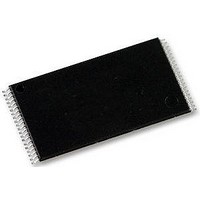
S29AL032D90TFI000 Spansion Inc., S29AL032D90TFI000 Datasheet - Page 43

S29AL032D90TFI000
Manufacturer Part Number
S29AL032D90TFI000
Description
Flash Memory IC
Manufacturer
Spansion Inc.
Specifications of S29AL032D90TFI000
Memory Size
32Mbit
Memory Configuration
4M X 8
Ic Interface Type
CFI, Parallel
Access Time
90ns
Supply Voltage Range
2.7 To 3.6 V
Memory Case Style
TSOP
No. Of Pins
40
Memory Type
Uniform Sector Flash
Interface Type
CFI
Rohs Compliant
Yes
Cell Type
NOR
Density
32Mb
Access Time (max)
90ns
Boot Type
Top
Address Bus
22/21Bit
Operating Supply Voltage (typ)
3/3.3V
Operating Temp Range
-40C to 85C
Package Type
TSOP
Sync/async
Asynchronous
Operating Temperature Classification
Industrial
Operating Supply Voltage (min)
2.7V
Operating Supply Voltage (max)
3.6V
Word Size
8/16Bit
Number Of Words
4M/2M
Supply Current
35mA
Mounting
Surface Mount
Pin Count
48
Lead Free Status / Rohs Status
Compliant
Available stocks
Company
Part Number
Manufacturer
Quantity
Price
12.2
January 19, 2007 S29AL032D_00_A9
RY/BY#: Ready/Busy#
Notes
1. VA = Valid address for programming. During a sector erase operation, a valid address is an address within any sector selected for
2. DQ7 should be rechecked even if DQ5 = 1 because DQ7 may change simultaneously with DQ5.
The RY/BY# is a dedicated, open-drain output pin that indicates whether an Embedded Algorithm is in
progress or complete. The RY/BY# status is valid after the rising edge of the final WE# pulse in the command
sequence. Since RY/BY# is an open-drain output, several RY/BY# pins can be tied together in parallel with a
pull-up resistor to V
If the output is low (Busy), the device is actively erasing or programming. (This includes programming in the
Erase Suspend mode.) If the output is high (Ready), the device is ready to read array data (including during
the Erase Suspend mode), or is in the standby mode.
Table 12.1 on page 44
50,
operations, respectively.
erasure. During chip erase, a valid address is any non-protected sector address.
Figure 17.5 on page 53
CC
.
shows the outputs for RY/BY#. Figures
D a t a
and
Figure 17.6 on page 53
S h e e t
Figure 12.1 Data# Polling Algorithm
No
S29AL032D
Read DQ7–DQ0
Read DQ7–DQ0
DQ7 = Data?
DQ7 = Data?
Addr = VA
Addr = VA
DQ5 = 1?
START
FAIL
No
Yes
No
shows RY/BY# for read, reset, program, and erase
Yes
Yes
Figure 17.1 on page
PASS
49,
Figure 17.2 on page
41


