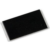
S29AL032D90TFI000 Spansion Inc., S29AL032D90TFI000 Datasheet - Page 46

S29AL032D90TFI000
Manufacturer Part Number
S29AL032D90TFI000
Description
Flash Memory IC
Manufacturer
Spansion Inc.
Specifications of S29AL032D90TFI000
Memory Size
32Mbit
Memory Configuration
4M X 8
Ic Interface Type
CFI, Parallel
Access Time
90ns
Supply Voltage Range
2.7 To 3.6 V
Memory Case Style
TSOP
No. Of Pins
40
Memory Type
Uniform Sector Flash
Interface Type
CFI
Rohs Compliant
Yes
Cell Type
NOR
Density
32Mb
Access Time (max)
90ns
Boot Type
Top
Address Bus
22/21Bit
Operating Supply Voltage (typ)
3/3.3V
Operating Temp Range
-40C to 85C
Package Type
TSOP
Sync/async
Asynchronous
Operating Temperature Classification
Industrial
Operating Supply Voltage (min)
2.7V
Operating Supply Voltage (max)
3.6V
Word Size
8/16Bit
Number Of Words
4M/2M
Supply Current
35mA
Mounting
Surface Mount
Pin Count
48
Lead Free Status / Rohs Status
Compliant
Available stocks
Company
Part Number
Manufacturer
Quantity
Price
12.6
12.7
Notes
1. DQ5 switches to ‘1’ when an Embedded Program or Embedded Erase operation exceeds the maximum timing limits. See
2. DQ7 and DQ2 require a valid address when reading status information. Refer to the appropriate subsection for further details.
44
Standard
Mode
Erase
Suspend
Mode
page 44
for more information.
DQ5: Exceeded Timing Limits
DQ3: Sector Erase Timer
Embedded Program Algorithm
Embedded Erase Algorithm
Reading within Erase
Suspended Sector
Reading within Non-Erase
Suspended Sector
Erase-Suspend-Program
DQ5 indicates whether the program or erase time has exceeded a specified internal pulse count limit. Under
these conditions DQ5 produces a 1. This is a failure condition that indicates the program or erase cycle was
not successfully completed.
The DQ5 failure condition may appear if the system tries to program a 1 to a location that is previously
programmed to 0. Only an erase operation can change a 0 back to a 1. Under this condition, the device
halts the operation, and when the operation has exceeded the timing limits, DQ5 produces a 1.
Under both these conditions, the system must issue the reset command to return the device to reading array
data.
After writing a sector erase command sequence, the system may read DQ3 to determine whether or not an
erase operation has begun. (The sector erase timer does not apply to the chip erase command.) If additional
sectors are selected for erasure, the entire time-out also applies after each additional sector erase command.
When the time-out is complete, DQ3 switches from 0 to 1. The system may ignore DQ3 if the system can
guarantee that the time between additional sector erase commands will always be less than 50 μs. See
also
After the sector erase command sequence is written, the system should read the status on DQ7 (Data#
Polling) or DQ6 (Toggle Bit I) to ensure that the device accepts the command sequence, and then read DQ3.
If DQ3 is 1, the internally controlled erase cycle has begun; all further commands (other than Erase Suspend)
are ignored until the erase operation is complete. If DQ3 is 0, the device accepts additional sector erase
commands. To ensure that the command has been accepted, the system software should check the status of
DQ3 prior to and following each subsequent sector erase command. If DQ3 is high on the second status
check, the last command might not have been accepted.
Operation
Sector Erase Command Sequence on page
Table 12.1 Write Operation Status
(Note 2)
DQ7#
DQ7#
DQ7
Data
0
1
S29AL032D
No toggle
Toggle
Toggle
Toggle
Data
DQ6
D a t a
35.
S h e e t
Table 12.1
(Note 1)
DQ5
Data
0
0
0
0
shows the outputs for DQ3.
DQ3
Data
N/A
N/A
N/A
1
DQ5: Exceeded Timing Limits on
S29AL032D_00_A9 January 19, 2007
No toggle
(Note 2)
Toggle
Toggle
Data
DQ2
N/A
RY/BY#
0
0
1
1
0


