LM2650M-ADJ National Semiconductor, LM2650M-ADJ Datasheet - Page 2
LM2650M-ADJ
Manufacturer Part Number
LM2650M-ADJ
Description
DC/DC CONVERTER, ADJ, 2650, SOIC24
Manufacturer
National Semiconductor
Datasheet
1.LM2650M-ADJ.pdf
(11 pages)
Specifications of LM2650M-ADJ
Primary Input Voltage
18V
No. Of Outputs
1
Output Voltage
16V
Output Current
3A
Voltage Regulator Case Style
SOIC
No. Of Pins
24
Operating Temperature Range
-40°C To +125°C
Svhc
No SVHC
Lead Free Status / RoHS Status
Lead free / RoHS Compliant
Available stocks
Company
Part Number
Manufacturer
Quantity
Price
Company:

Part Number:
LM2650M-ADJ
Manufacturer:
NS
Quantity:
1 438
Company:
Part Number:
LM2650M-ADJ
Manufacturer:
NATIONAL
Quantity:
425
Part Number:
LM2650M-ADJ
Manufacturer:
NS/国半
Quantity:
20 000
Company:
Part Number:
LM2650M-ADJ/NOPB
Manufacturer:
TI
Quantity:
15 540


www.national.com
1, 12
2
3, 4, 9, 10
5, 8
6, 7
11
13
14
15
16
17
18
19
20
21
22
23
24
Connection Diagram
Pin Descriptions
Pins
SUB: These pins make electrical contact with the substrate of the die. Ground them. For best thermal
performance, ground them to the same large, uninterrupted copper plane as the PGND pins.
SLEEP LOGIC: Use this logic input to select the conversion mode; low selects PWM, high selects sleep, and
high impedance (open) permits the LM2650 to move freely and automatically between the modes, using PWM
for moderate to heavy loads and sleep for light loads.
PGND: The ground return of the power stage. The power stage consists of the two power switches Q1 and
Q2, the gate drivers DH and DL, and the linear voltage regulators VRegH and VRegL. For best electrical and
thermal performance, ground these pins to a large, uninterrupted copper plane.
SW: The output node of the power stage. It swings from slightly below ground to slightly below the voltage to
PV
and to the point. Route all traces carrying signals well away from the SW traces.
PV
capacitors having low ESL and low ESR, and locate them close to the IC.
BOOT: The positive supply rail of the high-side gate driver DH. Connect a 0.1 µF capacitor from this node to
SW. Bootstrapping action creates a supply rail about 9V above that at PV
the gate of the NMOS power FET Q1. Overriding ensures low R
FB: The feedback input.
V
output node of this regulator. Bypass V
COMP: The inverting input of the error amplifier EA.
EA OUT: The output node of the error amplifier EA.
SS: The soft start node. Connect a capacitor from SS to GND.
GND: The ground return of the signal-level circuitry.
V
capacitor.
FREQ ADJ: The LM2650 switches at a nominal 90 kHz. Connect a resistor between FREQ ADJ and GND to
adjust the frequency up from the nominal. Use the graph under Typical performance Characteristics to select
the resistor.
SYNC: The synchronization input. If the switching frequency is to be synchronized with an external clock
signal, apply the clock signal here. Ground if not used.
SD: Use this logic input to control shutdown; pull low for operation, high for shutdown.
SLEEP OUT ADJ (SOA): The value of the resistor connected between SIA and ground programs the sleep-in
threshold. Higher values program lower thresholds.
SLEEP IN ADJ (SIA): The value of the resistor connected between SIA and ground programs the sleep-in
threshold. Higher values program lower thresholds.
DD
IN
IN
IN
: The positive supply rail of the internal 4V regulator. Bypass V
: An internal regulator steps the input voltage down to a 4V rail used by the signal-level circuitry. V
. To minimize the effects of switching noise on nearby circuitry, keep all traces originating from SW short
: The positive supply rail of the power stage. Bypass each PV
(Refer to the Block Diagrams)
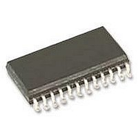
24-Lead Small Outline Package (M)
Order Number LM2650M-ADJ
See Package Number M24B
DD
Top View
to GND close to the IC with a 0.2 µF capacitor.
2
Description
DS012848-14
DS(on)
IN
IN
to GND close to the IC with a 0.1 µF
pin to PGND with a 0.1 µF capacitor. Use
.
IN
, and DH uses this rail to override
DD
is the
Related parts for LM2650M-ADJ
Image
Part Number
Description
Manufacturer
Datasheet
Request
R

Part Number:
Description:
IC CONVERTER SYNCH DC/DC 24-SOIC
Manufacturer:
National Semiconductor
Datasheet:


Part Number:
Description:
National Semiconductor [8-Bit D/A Converter]
Manufacturer:
National Semiconductor
Datasheet:
Part Number:
Description:
National Semiconductor [Media Coprocessor]
Manufacturer:
National Semiconductor
Datasheet:
Part Number:
Description:
Digitally Controlled Tone and Volume Circuit with Stereo Audio Power Amplifier, Microphone Preamp Stage and National 3D Sound
Manufacturer:
National Semiconductor
Datasheet:
Part Number:
Description:
Digitally Controlled Tone and Volume Circuit with Stereo Audio Power Amplifier, Microphone Preamp Stage and National 3D Sound
Manufacturer:
National Semiconductor
Datasheet:
Part Number:
Description:
AC97 Rev 2 Codec with Sample Rate Conversion and National 3D Sound
Manufacturer:
National Semiconductor
Part Number:
Description:
Manufacturer:
National Semiconductor
Datasheet:
Part Number:
Description:
Manufacturer:
National Semiconductor
Datasheet:
Part Number:
Description:
General Purpose, Low Voltage, Low Power, Rail-to-Rail Output Operational Amplifiers
Manufacturer:
National Semiconductor
Datasheet:
Part Number:
Description:
8-bit 20 MSPS flash A/D converter.
Manufacturer:
National Semiconductor
Datasheet:
Part Number:
Description:
Low Noise Quad Operational Amplifier
Manufacturer:
National Semiconductor
Datasheet:
Part Number:
Description:
Quad Differential Line Receivers
Manufacturer:
National Semiconductor
Datasheet:
Part Number:
Description:
Quad High Speed Trapezoidal? Bus Transceiver
Manufacturer:
National Semiconductor
Datasheet: